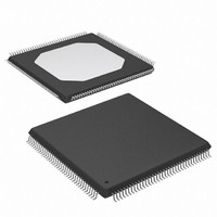
XCV50-6TQ144C Xilinx Inc, XCV50-6TQ144C Datasheet - Page 5

XCV50-6TQ144C
Manufacturer Part Number
XCV50-6TQ144C
Description
IC FPGA 2.5V C-TEMP 144-TQFP
Manufacturer
Xilinx Inc
Series
Virtex™r
Datasheet
1.XCV100-5PQ240C.pdf
(76 pages)
Specifications of XCV50-6TQ144C
Number Of Logic Elements/cells
1728
Number Of Labs/clbs
384
Total Ram Bits
32768
Number Of I /o
98
Number Of Gates
57906
Voltage - Supply
2.375 V ~ 2.625 V
Mounting Type
Surface Mount
Operating Temperature
0°C ~ 85°C
Package / Case
144-LQFP
Case
TQFP144
Dc
03+
Lead Free Status / RoHS Status
Contains lead / RoHS non-compliant
Available stocks
Company
Part Number
Manufacturer
Quantity
Price
Company:
Part Number:
XCV50-6TQ144C
Manufacturer:
XIL
Quantity:
1 238
Company:
Part Number:
XCV50-6TQ144C
Manufacturer:
XILINX
Quantity:
988
DS003-2 (v2.8.1) December 9, 2002
Architectural Description
Virtex Array
The Virtex user-programmable gate array, shown in
Figure
figurable logic blocks (CLBs) and input/output blocks
(IOBs).
•
•
CLBs interconnect through a general routing matrix (GRM).
The GRM comprises an array of routing switches located at
the intersections of horizontal and vertical routing channels.
Each CLB nests into a VersaBlock™ that also provides local
routing resources to connect the CLB to the GRM.
The VersaRing™ I/O interface provides additional routing
resources around the periphery of the device. This routing
improves I/O routability and facilitates pin locking.
The Virtex architecture also includes the following circuits
that connect to the GRM.
•
•
•
Values stored in static memory cells control the configurable
logic elements and interconnect resources. These values
load into the memory cells on power-up, and can reload if
necessary to change the function of the device.
Input/Output Block
The Virtex IOB,
outputs that support a wide variety of I/O signalling stan-
dards, see
The three IOB storage elements function either as edge-trig-
gered D-type flip-flops or as level sensitive latches. Each
IOB has a clock signal (CLK) shared by the three flip-flops
and independent clock enable signals for each flip-flop.
In addition to the CLK and CE control signals, the three
flip-flops share a Set/Reset (SR). For each flip-flop, this sig-
nal can be independently configured as a synchronous Set,
a synchronous Reset, an asynchronous Preset, or an asyn-
chronous Clear.
DS003-2 (v2.8.1) December 9, 2002
Product Specification
© 1999-2002 Xilinx, Inc. All rights reserved. All Xilinx trademarks, registered trademarks, patents, and disclaimers are as listed at http://www.xilinx.com/legal.htm.
CLBs provide the functional elements for constructing
logic
IOBs provide the interface between the package pins
and the CLBs
Dedicated block memories of 4096 bits each
Clock DLLs for clock-distribution delay compensation
and clock domain control
3-State buffers (BUFTs) associated with each CLB that
drive dedicated segmentable horizontal routing
resources
1, comprises two major configurable elements: con-
All other trademarks and registered trademarks are the property of their respective owners. All specifications are subject to change without notice.
Table
1.
Figure
2, features SelectIO™ inputs and
R
0
0
www.xilinx.com
1-800-255-7778
0
Virtex™ 2.5 V
Field Programmable Gate Arrays
Product Specification
The output buffer and all of the IOB control signals have
independent polarity controls.
All pads are protected against damage from electrostatic
discharge (ESD) and from over-voltage transients. Two
forms of over-voltage protection are provided, one that per-
mits 5 V compliance, and one that does not. For 5 V compli-
ance, a Zener-like structure connected to ground turns on
when the output rises to approximately 6.5 V. When PCI
3.3 V compliance is required, a conventional clamp diode is
connected to the output supply voltage, V
Optional pull-up and pull-down resistors and an optional
weak-keeper circuit are attached to each pad. Prior to con-
figuration, all pins not involved in configuration are forced
into their high-impedance state. The pull-down resistors and
the weak-keeper circuits are inactive, but inputs can option-
ally be pulled up.
The activation of pull-up resistors prior to configuration is
controlled on a global basis by the configuration mode pins.
If the pull-up resistors are not activated, all the pins will float.
Consequently, external pull-up or pull-down resistors must
be provided on pins required to be at a well-defined logic
level prior to configuration.
All Virtex IOBs support IEEE 1149.1-compatible boundary
scan testing.
DLL
DLL
Figure 1: Virtex Architecture Overview
VersaRing
VersaRing
IOBs
CLBs
IOBs
CCO
.
vao_b.eps
Module 2 of 4
DLL
DLL
1


