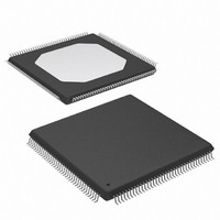
XCV50-6TQ144C Xilinx Inc, XCV50-6TQ144C Datasheet - Page 40

XCV50-6TQ144C
Manufacturer Part Number
XCV50-6TQ144C
Description
IC FPGA 2.5V C-TEMP 144-TQFP
Manufacturer
Xilinx Inc
Series
Virtex™r
Datasheet
1.XCV100-5PQ240C.pdf
(76 pages)
Specifications of XCV50-6TQ144C
Number Of Logic Elements/cells
1728
Number Of Labs/clbs
384
Total Ram Bits
32768
Number Of I /o
98
Number Of Gates
57906
Voltage - Supply
2.375 V ~ 2.625 V
Mounting Type
Surface Mount
Operating Temperature
0°C ~ 85°C
Package / Case
144-LQFP
Case
TQFP144
Dc
03+
Lead Free Status / RoHS Status
Contains lead / RoHS non-compliant
Available stocks
Company
Part Number
Manufacturer
Quantity
Price
Company:
Part Number:
XCV50-6TQ144C
Manufacturer:
XIL
Quantity:
1 238
Company:
Part Number:
XCV50-6TQ144C
Manufacturer:
XILINX
Quantity:
988
Virtex™ 2.5 V Field Programmable Gate Arrays
Block RAM Switching Characteristics
TBUF Switching Characteristics
JTAG Test Access Port Switching Characteristics
Module 3 of 4
16
Notes:
1.
Sequential Delays
Clock CLK to DOUT output
Setup and Hold Times before/after Clock CLK
ADDR inputs
DIN inputs
EN input
RST input
WEN input
Clock CLK
Minimum Pulse Width, High
Minimum Pulse Width, Low
CLKA -> CLKB setup time for different ports
Combinatorial Delays
IN input to OUT output
TRI input to OUT output high-impedance
TRI input to valid data on OUT output
TMS and TDI Setup times before TCK
TMS and TDI Hold times after TCK
Output delay from clock TCK to output TDO
Maximum TCK clock frequency
A Zero "0" Hold Time listing indicates no hold time or a negative hold time. Negative values can not be guaranteed "best-case", but
if a "0" is listed, there is no positive hold time.
Description
Description
Description
(1)
www.xilinx.com
1-800-255-7778
T
T
T
T
T
BWCK
BDCK
BRCK
BACK
BECK
Symbol
T
T
T
T
T
T
T
Symbol
BPWH
BPWL
BCKO
BCCS
TCKTDO
TAPTCK
TCKTAP
F
/T
/T
/T
/T
/T
Symbol
TCK
BCKA
BCKD
BCKE
BCKR
BCKW
T
T
T
OFF
ON
IO
0.6 / 0
0.6 / 0
1.3 / 0
1.3 / 0
1.2 / 0
Min
1.7
0.8
0.8
0.05
0.05
11.0
Min
Setup Time / Hold Time
4.0
2.0
33
-6
0
1.2 / 0
1.2 / 0
2.6 / 0
2.5 / 0
2.3 / 0
Speed Grade
Speed Grade
3.4
1.5
1.5
3.0
-6
Speed Grade
0.09
0.09
-6
0
11.0
4.0
2.0
33
-5
DS003-3 (v3.2) September 10, 2002
Production Product Specification
1.3 / 0
1.3 / 0
3.0 / 0
2.7 / 0
2.6 / 0
0.10
0.10
3.8
1.7
1.7
3.5
-5
-5
0
11.0
4.0
2.0
33
-4
1.5 / 0
1.5 / 0
3.4 / 0
3.2 / 0
3.0 / 0
0.11
0.11
4.3
2.0
2.0
4.0
-4
-4
0
MHz, max
ns, max
ns, min
ns, min
Units
ns, max
ns, max
ns, max
ns, max
ns, min
ns, min
ns, min
ns, min
ns, min
ns, min
ns, min
ns, min
Units
Units
R


