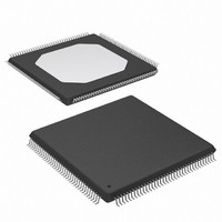
XCV50-6TQ144C Xilinx Inc, XCV50-6TQ144C Datasheet - Page 28

XCV50-6TQ144C
Manufacturer Part Number
XCV50-6TQ144C
Description
IC FPGA 2.5V C-TEMP 144-TQFP
Manufacturer
Xilinx Inc
Series
Virtex™r
Datasheet
1.XCV100-5PQ240C.pdf
(76 pages)
Specifications of XCV50-6TQ144C
Number Of Logic Elements/cells
1728
Number Of Labs/clbs
384
Total Ram Bits
32768
Number Of I /o
98
Number Of Gates
57906
Voltage - Supply
2.375 V ~ 2.625 V
Mounting Type
Surface Mount
Operating Temperature
0°C ~ 85°C
Package / Case
144-LQFP
Case
TQFP144
Dc
03+
Lead Free Status / RoHS Status
Contains lead / RoHS non-compliant
Available stocks
Company
Part Number
Manufacturer
Quantity
Price
Company:
Part Number:
XCV50-6TQ144C
Manufacturer:
XIL
Quantity:
1 238
Company:
Part Number:
XCV50-6TQ144C
Manufacturer:
XILINX
Quantity:
988
Virtex™ 2.5 V Field Programmable Gate Arrays
Power-On Power Supply Requirements
Xilinx FPGAs require a certain amount of supply current during power-on to insure proper device operation. The actual
current consumed depends on the power-on ramp rate of the power supply. This is the time required to reach the nominal
power supply voltage of the device
voltage in 2 ms) and is lowest at the slowest allowed ramp rate (0 V to nominal voltage in 50 ms). For more details on power
supply requirements, see Application Note XAPP158
DC Input and Output Levels
Values for V
recommended operating conditions at the V
to ensure that all standards meet their specifications. The selected standards are tested at minimum V
with the respective V
Module 3 of 4
4
Notes:
1.
2.
3.
Notes:
1.
2.
3.
Virtex Family, Commercial Grade
Virtex Family, Industrial Grade
LVTTL
LVCMOS2
PCI, 3.3 V
PCI, 5.0 V
GTL
GTL+
HSTL I
HSTL III
HSTL IV
SSTL3 I
SSTL3 II
SSTL2 I
SSTL2 II
CTT
AGP
Input/Output
Standard
Ramp rate used for this specification is from 0 - 2.7 VDC. Peak current occurs on or near the internal power-on reset threshold of
1.0V and lasts for less than 3 ms.
Devices are guaranteed to initialize properly with the minimum current available from the power supply as noted above.
Larger currents can result if ramp rates are forced to be faster.
V
Tested according to the relevant specifications.
DC input and output levels for HSTL18 (HSTL I/O standard with V
www.xilinx.com.
OL
(1)
(3)
and V
IL
OH
and V
for lower drive currents are sample tested.
V, min
– 0.5
– 0.5
– 0.5
– 0.5
– 0.5
– 0.5
– 0.5
– 0.5
– 0.5
– 0.5
– 0.5
– 0.5
– 0.5
– 0.5
– 0.5
OL
IH
Product
are recommended input voltages. Values for I
and V
V
44% V
V
OH
V
V
V
V
V
V
V
V
V
V
IL
REF
REF
REF
REF
REF
REF
REF
REF
REF
REF
REF
V, max
voltage levels shown. Other standards are sample tested.
0.8
0.8
.7
– 0.05
(1)
– 0.1
– 0.1
– 0.1
– 0.1
– 0.2
– 0.2
– 0.2
– 0.2
– 0.2
– 0.2
CCINT
from 0 V. The current is highest at the fastest suggested ramp rate (0 V to nominal
OL
60% V
V
V
V
V
V
V
V
V
V
V
V
REF
REF
REF
REF
REF
REF
REF
REF
REF
REF
REF
and V
V, min
2.0
1.7
2.0
+ 0.05
+ 0.1
+ 0.1
+ 0.1
+ 0.1
+ 0.2
+ 0.2
+ 0.2
+ 0.2
+ 0.2
+ 0.2
CCINT
OH
on www.xilinx.com.
www.xilinx.com
1-800-255-7778
V
test points. Only selected standards are tested. These are chosen
Minimum required current supply
Minimum required current supply
IH
V
CCO
V, max
5.5
5.5
5.5
3.6
3.6
3.6
3.6
3.6
3.6
3.6
3.6
3.6
3.6
3.6
CCO
+ 0.5
Description
of 1.8 V) are provided in an HSTL white paper on
OL
V
V
and I
V
V
V
10% V
10% V
REF
REF
REF
REF
REF
V, Max
0.55
V
0.4
0.4
0.4
0.6
0.4
0.4
0.4
OH
(2)
OL
– 0.61 V
– 0.80 V
– 0.6
– 0.8
– 0.4
CCO
CCO
are guaranteed output currents over the
V
V
V
90% V
V
V
V
90% V
REF
REF
CCO
CCO
CCO
REF
REF
REF
DS003-3 (v3.2) September 10, 2002
V, Min
Production Product Specification
V
2.4
1.9
2.4
n/a
n/a
OH
+ 0.61
+ 0.80
+ 0.6
+ 0.8
+ 0.4
Current Requirement
– 0.4
– 0.4
– 0.4
CCO
CCO
CCO
Note 2
Note 2
Note 2
500 mA
15.2
mA
I
7.6
24
12
40
36
24
48
16
for each standard
OL
2 A
8
8
8
Note 2
Note 2
Note 2
–15.2
–7.6
mA
–24
–12
–16
I
n/a
n/a
–8
–8
–8
–8
–8
OH
(1,3)
R


