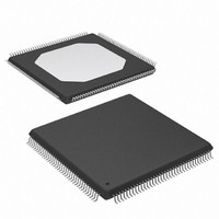
XCV50-6TQ144C Xilinx Inc, XCV50-6TQ144C Datasheet - Page 9

XCV50-6TQ144C
Manufacturer Part Number
XCV50-6TQ144C
Description
IC FPGA 2.5V C-TEMP 144-TQFP
Manufacturer
Xilinx Inc
Series
Virtex™r
Datasheet
1.XCV100-5PQ240C.pdf
(76 pages)
Specifications of XCV50-6TQ144C
Number Of Logic Elements/cells
1728
Number Of Labs/clbs
384
Total Ram Bits
32768
Number Of I /o
98
Number Of Gates
57906
Voltage - Supply
2.375 V ~ 2.625 V
Mounting Type
Surface Mount
Operating Temperature
0°C ~ 85°C
Package / Case
144-LQFP
Case
TQFP144
Dc
03+
Lead Free Status / RoHS Status
Contains lead / RoHS non-compliant
Available stocks
Company
Part Number
Manufacturer
Quantity
Price
Company:
Part Number:
XCV50-6TQ144C
Manufacturer:
XIL
Quantity:
1 238
Company:
Part Number:
XCV50-6TQ144C
Manufacturer:
XILINX
Quantity:
988
Additional Logic
The F5 multiplexer in each slice combines the function gen-
erator outputs. This combination provides either a function
generator that can implement any 5-input function, a 4:1
multiplexer, or selected functions of up to nine inputs.
Similarly, the F6 multiplexer combines the outputs of all four
function generators in the CLB by selecting one of the
F5-multiplexer outputs. This permits the implementation of
any 6-input function, an 8:1 multiplexer, or selected func-
tions of up to 19 inputs.
Each CLB has four direct feedthrough paths, one per LC.
These paths provide extra data input lines or additional local
routing that does not consume logic resources.
Arithmetic Logic
Dedicated carry logic provides fast arithmetic carry capabil-
ity for high-speed arithmetic functions. The Virtex CLB sup-
ports two separate carry chains, one per Slice. The height
of the carry chains is two bits per CLB.
The arithmetic logic includes an XOR gate that allows a
1-bit full adder to be implemented within an LC. In addition,
a dedicated AND gate improves the efficiency of multiplier
implementation.
The dedicated carry path can also be used to cascade func-
tion generators for implementing wide logic functions.
BUFTs
Each Virtex CLB contains two 3-state drivers (BUFTs) that
can drive on-chip busses. See Dedicated
Each Virtex BUFT has an independent 3-state control pin
and an independent input pin.
DS003-2 (v2.8.1) December 9, 2002
Product Specification
R
F5IN
CLK
G4
G3
G2
G1
BY
BX
SR
CE
F4
F3
F2
F1
WE
CK
A4
I3
I2
I1
I0
I3
I2
I1
I0
Figure 5: Detailed View of VIrtex Slice
Routing, page
WSO
WSH
WE
WE
LUT
LUT
BX
BY DG
DI
DI
DI
O
O
www.xilinx.com
1-800-255-7778
0
1
0
1
7.
COUT
CY
CY
CIN
Block SelectRAM
Virtex FPGAs incorporate several large block SelectRAM
memories. These complement the distributed LUT
SelectRAMs that provide shallow RAM structures imple-
mented in CLBs.
Block SelectRAM memory blocks are organized in columns.
All Virtex devices contain two such columns, one along
each vertical edge. These columns extend the full height of
the chip. Each memory block is four CLBs high, and conse-
quently, a Virtex device 64 CLBs high contains 16 memory
blocks per column, and a total of 32 blocks.
Table 3
is available in each Virtex device.
Table 3: Virtex Block SelectRAM Amounts
XCV1000
XCV100
XCV150
XCV200
XCV300
XCV400
XCV600
XCV800
F5
Device
XCV50
F6
shows the amount of block SelectRAM memory that
Virtex™ 2.5 V Field Programmable Gate Arrays
# of Blocks
viewslc4.eps
10
12
14
16
20
24
28
32
8
EC
EC
D
D
INIT
REV
INIT
REV
Q
Q
Total Block SelectRAM Bits
YB
X
YQ
XB
F5
XQ
Y
114,688
131,072
32,768
40,960
49,152
57,344
65,536
81,920
98,304
Module 2 of 4
5


