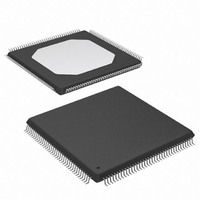
XCV50-6TQ144C Xilinx Inc, XCV50-6TQ144C Datasheet - Page 23

XCV50-6TQ144C
Manufacturer Part Number
XCV50-6TQ144C
Description
IC FPGA 2.5V C-TEMP 144-TQFP
Manufacturer
Xilinx Inc
Series
Virtex™r
Datasheet
1.XCV100-5PQ240C.pdf
(76 pages)
Specifications of XCV50-6TQ144C
Number Of Logic Elements/cells
1728
Number Of Labs/clbs
384
Total Ram Bits
32768
Number Of I /o
98
Number Of Gates
57906
Voltage - Supply
2.375 V ~ 2.625 V
Mounting Type
Surface Mount
Operating Temperature
0°C ~ 85°C
Package / Case
144-LQFP
Case
TQFP144
Dc
03+
Lead Free Status / RoHS Status
Contains lead / RoHS non-compliant
Available stocks
Company
Part Number
Manufacturer
Quantity
Price
Company:
Part Number:
XCV50-6TQ144C
Manufacturer:
XIL
Quantity:
1 238
Company:
Part Number:
XCV50-6TQ144C
Manufacturer:
XILINX
Quantity:
988
Data Stream Format
Virtex devices are configured by sequentially loading
frames of data.
required to configure each device. For more detailed infor-
mation, see application note XAPP151 “Virtex Configura-
tion Architecture Advanced Users Guide”.
Table 11: Virtex Bit-Stream Lengths
Revision History
DS003-2 (v2.8.1) December 9, 2002
Product Specification
11/98
01/99
02/99
05/99
05/99
07/99
09/99
01/00
Date
XCV1000
XCV100
XCV150
XCV200
XCV300
XCV400
XCV600
XCV800
Device
XCV50
R
Table 11
Version
1.0
1.2
1.3
1.4
1.5
1.6
1.7
1.8
# of Configuration Bits
lists the total number of bits
Initial Xilinx release.
Updated package drawings and specs.
Update of package drawings, updated specifications.
Addition of package drawings and specifications.
Replaced FG 676 & FG680 package drawings.
Changed Boundary Scan Information and changed Figure 11, Boundary Scan Bit
Sequence. Updated IOB Input & Output delays. Added Capacitance info for different I/O
Standards. Added 5 V tolerant information. Added DLL Parameters and waveforms and
new Pin-to-pin Input and Output Parameter tables for Global Clock Input to Output and
Setup and Hold. Changed Configuration Information including Figures 12, 14, 17 & 19.
Added device-dependent listings for quiescent currents ICCINTQ and ICCOQ. Updated
IOB Input and Output Delays based on default standard of LVTTL, 12 mA, Fast Slew Rate.
Added IOB Input Switching Characteristics Standard Adjustments.
Speed grade update to preliminary status, Power-on specification and Clock-to-Out
Minimums additions, “0” hold time listing explanation, quiescent current listing update, and
Figure 6 ADDRA input label correction. Added T
Update to speed.txt file 1.96. Corrections for CRs 111036,111137, 112697, 115479,
117153, 117154, and 117612. Modified notes for Recommended Operating Conditions
(voltage and temperature). Changed Bank information for V
1,040,096
1,335,840
1,751,808
2,546,048
3,607,968
4,715,616
6,127,744
559,200
781,216
www.xilinx.com
1-800-255-7778
Readback
The configuration data stored in the Virtex configuration
memory can be readback for verification. Along with the
configuration data it is possible to readback the contents all
flip-flops/latches, LUTRAMs, and block RAMs. This capabil-
ity is used for real-time debugging.
For more detailed information, see Application Note
XAPP138: Virtex FPGA Series Configuration and Readback,
available online at
Revision
Virtex™ 2.5 V Field Programmable Gate Arrays
IJITCC
www.xilinx.com
parameter, changed T
CCO
in CS144 package on p.43.
.
OJIT
to T
Module 2 of 4
OPHASE
19
.


