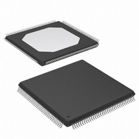
XCV50-6TQ144C Xilinx Inc, XCV50-6TQ144C Datasheet - Page 8

XCV50-6TQ144C
Manufacturer Part Number
XCV50-6TQ144C
Description
IC FPGA 2.5V C-TEMP 144-TQFP
Manufacturer
Xilinx Inc
Series
Virtex™r
Datasheet
1.XCV100-5PQ240C.pdf
(76 pages)
Specifications of XCV50-6TQ144C
Number Of Logic Elements/cells
1728
Number Of Labs/clbs
384
Total Ram Bits
32768
Number Of I /o
98
Number Of Gates
57906
Voltage - Supply
2.375 V ~ 2.625 V
Mounting Type
Surface Mount
Operating Temperature
0°C ~ 85°C
Package / Case
144-LQFP
Case
TQFP144
Dc
03+
Lead Free Status / RoHS Status
Contains lead / RoHS non-compliant
Available stocks
Company
Part Number
Manufacturer
Quantity
Price
Company:
Part Number:
XCV50-6TQ144C
Manufacturer:
XIL
Quantity:
1 238
Company:
Part Number:
XCV50-6TQ144C
Manufacturer:
XILINX
Quantity:
988
Virtex™ 2.5 V Field Programmable Gate Arrays
more I/O pins convert to V
a superset of the V
possible to design a PCB that permits migration to a larger
device if necessary. All the V
anticipated must be connected to the V
used for I/O.
In smaller devices, some V
do not connect within the package. These unconnected pins
can be left unconnected externally, or can be connected to
the V
necessary.
In TQ144 and PQ/HQ240 packages, all V
bonded together internally, and consequently the same
V
CS144 package, bank pairs that share a side are intercon-
nected internally, permitting four choices for V
cases, the V
banks, and can be used as described previously.
Configurable Logic Block
The basic building block of the Virtex CLB is the logic cell
(LC). An LC includes a 4-input function generator, carry
logic, and a storage element. The output from the function
generator in each LC drives both the CLB output and the D
input of the flip-flop. Each Virtex CLB contains four LCs,
organized in two similar slices, as shown in
Figure 5
In addition to the four basic LCs, the Virtex CLB contains
logic that combines function generators to provide functions
Module 2 of 4
4
CCO
CCO
voltage must be connected to all of them. In the
shows a more detailed view of a single slice.
voltage to permit migration to a larger device if
REF
pins remain internally connected as eight
G2
G1
G4
G3
BY
F2
F1
BX
F4
F3
REF
pins used for smaller devices, it is
REF
LUT
LUT
CCO
REF
pins. Since these are always
pins used in larger devices
pins for the largest device
Carry &
Control
Carry &
Control
COUT
REF
CIN
voltage, and not
Figure
CCO
Figure 4: 2-Slice Virtex CLB
CCO
D
EC
D
EC
RC
RC
SP
SP
Slice 1
pins are
. In both
4.
Q
Q
www.xilinx.com
1-800-255-7778
YB
YQ
XB
XQ
X
Y
G4
G3
F2
F1
G2
G1
F4
F3
BX
BY
of five or six inputs. Consequently, when estimating the
number of system gates provided by a given device, each
CLB counts as 4.5 LCs.
Look-Up Tables
Virtex function generators are implemented as 4-input
look-up tables (LUTs). In addition to operating as a function
generator, each LUT can provide a 16 x 1-bit synchronous
RAM. Furthermore, the two LUTs within a slice can be com-
bined to create a 16 x 2-bit or 32 x 1-bit synchronous RAM,
or a 16x1-bit dual-port synchronous RAM.
The Virtex LUT can also provide a 16-bit shift register that is
ideal for capturing high-speed or burst-mode data. This
mode can also be used to store data in applications such as
Digital Signal Processing.
Storage Elements
The storage elements in the Virtex slice can be configured
either as edge-triggered D-type flip-flops or as level-sensi-
tive latches. The D inputs can be driven either by the func-
tion generators within the slice or directly from slice inputs,
bypassing the function generators.
In addition to Clock and Clock Enable signals, each Slice
has synchronous set and reset signals (SR and BY). SR
forces a storage element into the initialization state speci-
fied for it in the configuration. BY forces it into the opposite
state. Alternatively, these signals can be configured to oper-
ate asynchronously. All of the control signals are indepen-
dently invertible, and are shared by the two flip-flops within
the slice.
LUT
LUT
Carry &
Control
Carry &
Control
COUT
CIN
DS003-2 (v2.8.1) December 9, 2002
D
EC
D
EC
RC
SP
RC
SP
Slice 0
Q
Q
slice_b.eps
XB
Product Specification
YQ
X
XQ
YB
Y
R


