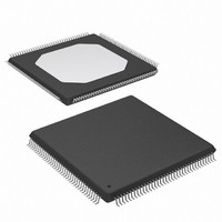
XCV50-6TQ144C Xilinx Inc, XCV50-6TQ144C Datasheet - Page 41

XCV50-6TQ144C
Manufacturer Part Number
XCV50-6TQ144C
Description
IC FPGA 2.5V C-TEMP 144-TQFP
Manufacturer
Xilinx Inc
Series
Virtex™r
Datasheet
1.XCV100-5PQ240C.pdf
(76 pages)
Specifications of XCV50-6TQ144C
Number Of Logic Elements/cells
1728
Number Of Labs/clbs
384
Total Ram Bits
32768
Number Of I /o
98
Number Of Gates
57906
Voltage - Supply
2.375 V ~ 2.625 V
Mounting Type
Surface Mount
Operating Temperature
0°C ~ 85°C
Package / Case
144-LQFP
Case
TQFP144
Dc
03+
Lead Free Status / RoHS Status
Contains lead / RoHS non-compliant
Available stocks
Company
Part Number
Manufacturer
Quantity
Price
Company:
Part Number:
XCV50-6TQ144C
Manufacturer:
XIL
Quantity:
1 238
Company:
Part Number:
XCV50-6TQ144C
Manufacturer:
XILINX
Quantity:
988
Virtex Pin-to-Pin Output Parameter Guidelines
All devices are 100% functionally tested. Listed below are representative values for typical pin locations and normal clock
loading. Values are expressed in nanoseconds unless otherwise noted.
Global Clock Input to Output Delay for LVTTL, 12 mA, Fast Slew Rate, with DLL
Global Clock Input-to-Output Delay for LVTTL, 12 mA, Fast Slew Rate, without DLL
DS003-3 (v3.2) September 10, 2002
Production Product Specification
Notes:
1.
2.
3.
Notes:
1.
2.
LVTTL Global Clock Input to Output Delay using
Output Flip-flop, 12 mA, Fast Slew Rate, with DLL.
For data output with different standards, adjust
delays with the values shown in Output Delay
Adjustments.
LVTTL Global Clock Input to Output Delay using
Output Flip-flop, 12 mA, Fast Slew Rate, without DLL.
For data output with different standards, adjust
delays with the values shown in Input and Output
Delay Adjustments.
For I/O standards requiring V
GTL+, SSTL, HSTL, CTT, and AGO, an additional
600 ps must be added.
Listed above are representative values where one global clock input drives one vertical clock line in each accessible column, and
where all accessible IOB and CLB flip-flops are clocked by the global clock net.
Output timing is measured at 1.4 V with 35 pF external capacitive load for LVTTL. The 35 pF load does not apply to the Min values.
For other I/O standards and different loads, see
DLL output jitter is already included in the timing calculation.
Listed above are representative values where one global clock input drives one vertical clock line in each accessible column, and
where all accessible IOB and CLB flip-flops are clocked by the global clock net.
Output timing is measured at 1.4 V with 35 pF external capacitive load for LVTTL. The 35 pF load does not apply to the Min values.
For other I/O standards and different loads, see
R
Description
Description
REF
, such as GTL,
Table 2
Table 2
www.xilinx.com
T
1-800-255-7778
and
and
Symbol
ICKOFDLL
Symbol
T
ICKOF
Table
Table
3.
3.
XCV1000
XCV100
XCV150
XCV200
XCV300
XCV400
XCV600
XCV800
XCV1000
Device
XCV50
XCV100
XCV150
XCV200
XCV300
XCV400
XCV600
XCV800
Device
XCV50
Virtex™ 2.5 V Field Programmable Gate Arrays
Min
1.0
1.0
1.0
1.0
1.0
1.0
1.0
1.0
1.0
Min
1.5
1.5
1.5
1.5
1.5
1.6
1.6
1.5
1.7
Speed Grade
Speed Grade
3.1
3.1
3.1
3.1
3.1
3.1
3.1
3.1
3.1
-6
4.6
4.6
4.7
4.7
4.7
4.8
4.9
4.9
5.0
-6
3.3
3.3
3.3
3.3
3.3
3.3
3.3
3.3
3.3
-5
5.1
5.2
5.2
5.2
5.3
5.4
5.5
5.6
5.1
-5
3.6
3.6
3.6
3.6
3.6
3.6
3.6
3.6
3.6
5.7
5.7
5.8
5.8
5.9
6.0
6.0
6.2
6.3
-4
-4
Module 3 of 4
ns, max
ns, max
ns, max
ns, max
ns, max
ns, max
ns, max
ns, max
ns, max
ns, max
ns, max
ns, max
ns, max
ns, max
ns, max
ns, max
ns, max
ns, max
Units
Units
17


