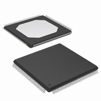
XCV50-6TQ144C Xilinx Inc, XCV50-6TQ144C Datasheet - Page 11

XCV50-6TQ144C
Manufacturer Part Number
XCV50-6TQ144C
Description
IC FPGA 2.5V C-TEMP 144-TQFP
Manufacturer
Xilinx Inc
Series
Virtex™r
Datasheet
1.XCV100-5PQ240C.pdf
(76 pages)
Specifications of XCV50-6TQ144C
Number Of Logic Elements/cells
1728
Number Of Labs/clbs
384
Total Ram Bits
32768
Number Of I /o
98
Number Of Gates
57906
Voltage - Supply
2.375 V ~ 2.625 V
Mounting Type
Surface Mount
Operating Temperature
0°C ~ 85°C
Package / Case
144-LQFP
Case
TQFP144
Dc
03+
Lead Free Status / RoHS Status
Contains lead / RoHS non-compliant
Available stocks
Company
Part Number
Manufacturer
Quantity
Price
Company:
Part Number:
XCV50-6TQ144C
Manufacturer:
XIL
Quantity:
1 238
Company:
Part Number:
XCV50-6TQ144C
Manufacturer:
XILINX
Quantity:
988
General Purpose Routing
Most Virtex signals are routed on the general purpose rout-
ing, and consequently, the majority of interconnect
resources are associated with this level of the routing hier-
archy. The general routing resources are located in horizon-
tal and vertical routing channels associated with the rows
and columns CLBs. The general-purpose routing resources
are listed below.
•
•
•
Global Routing
Global Routing resources distribute clocks and other sig-
nals with very high fanout throughout the device. Virtex
devices include two tiers of global routing resources
referred to as primary global and secondary local clock rout-
ing resources.
•
DS003-2 (v2.8.1) December 9, 2002
Product Specification
Adjacent to each CLB is a General Routing Matrix
(GRM). The GRM is the switch matrix through which
horizontal and vertical routing resources connect, and
is also the means by which the CLB gains access to
the general purpose routing.
24 single-length lines route GRM signals to adjacent
GRMs in each of the four directions.
12 buffered Hex lines route GRM signals to another
GRMs six-blocks away in each one of the four
directions. Organized in a staggered pattern, Hex lines
can be driven only at their endpoints. Hex-line signals
can be accessed either at the endpoints or at the
midpoint (three blocks from the source). One third of
the Hex lines are bidirectional, while the remaining
ones are uni-directional.
The primary global routing resources are four
dedicated global nets with dedicated input pins that are
designed to distribute high-fanout clock signals with
minimal skew. Each global clock net can drive all CLB,
IOB, and block RAM clock pins. The primary global
nets can only be driven by global buffers. There are
four global buffers, one for each global net.
R
CLB
Figure 8: BUFT Connections to Dedicated Horizontal Bus Lines
CLB
www.xilinx.com
1-800-255-7778
CLB
•
I/O Routing
Virtex devices have additional routing resources around
their periphery that form an interface between the CLB array
and the IOBs. This additional routing, called the VersaRing,
facilitates pin-swapping and pin-locking, such that logic
redesigns can adapt to existing PCB layouts. Time-to-mar-
ket is reduced, since PCBs and other system components
can be manufactured while the logic design is still in
progress.
Dedicated Routing
Some classes of signal require dedicated routing resources
to maximize performance. In the Virtex architecture, dedi-
cated routing resources are provided for two classes of sig-
nal.
•
•
•
Clock Distribution
Virtex provides high-speed, low-skew clock distribution
through the primary global routing resources described
above. A typical clock distribution net is shown in
Four global buffers are provided, two at the top center of the
device and two at the bottom center. These drive the four
primary global nets that in turn drive any clock pin.
12 Longlines are buffered, bidirectional wires that
distribute signals across the device quickly and
efficiently. Vertical Longlines span the full height of the
device, and horizontal ones span the full width of the
device.
Horizontal routing resources are provided for on-chip
3-state busses. Four partitionable bus lines are
provided per CLB row, permitting multiple busses
within a row, as shown in
Two dedicated nets per CLB propagate carry signals
vertically to the adjacent CLB.
The secondary local clock routing resources consist of
24 backbone lines, 12 across the top of the chip and 12
across bottom. From these lines, up to 12 unique
signals per column can be distributed via the 12
longlines in the column. These secondary resources
are more flexible than the primary resources since they
are not restricted to routing only to clock pins.
Virtex™ 2.5 V Field Programmable Gate Arrays
CLB
Figure
buft_c.eps
Tri-State
8.
Lines
Module 2 of 4
Figure
9.
7


