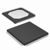
XCV50-6TQ144C Xilinx Inc, XCV50-6TQ144C Datasheet - Page 13

XCV50-6TQ144C
Manufacturer Part Number
XCV50-6TQ144C
Description
IC FPGA 2.5V C-TEMP 144-TQFP
Manufacturer
Xilinx Inc
Series
Virtex™r
Datasheet
1.XCV100-5PQ240C.pdf
(76 pages)
Specifications of XCV50-6TQ144C
Number Of Logic Elements/cells
1728
Number Of Labs/clbs
384
Total Ram Bits
32768
Number Of I /o
98
Number Of Gates
57906
Voltage - Supply
2.375 V ~ 2.625 V
Mounting Type
Surface Mount
Operating Temperature
0°C ~ 85°C
Package / Case
144-LQFP
Case
TQFP144
Dc
03+
Lead Free Status / RoHS Status
Contains lead / RoHS non-compliant
Available stocks
Company
Part Number
Manufacturer
Quantity
Price
Company:
Part Number:
XCV50-6TQ144C
Manufacturer:
XIL
Quantity:
1 238
Company:
Part Number:
XCV50-6TQ144C
Manufacturer:
XILINX
Quantity:
988
In addition to the test instructions outlined above, the
boundary-scan circuitry can be used to configure the
FPGA, and also to read back the configuration data.
Figure 10
logic. It includes three bits of Data Register per IOB, the
IEEE 1149.1 Test Access Port controller, and the Instruction
Register with decodes.
Instruction Set
The Virtex Series boundary scan instruction set also
includes instructions to configure the device and read back
configuration data (CFG_IN, CFG_OUT, and JSTART). The
complete instruction set is coded as shown in
Data Registers
The primary data register is the boundary scan register. For
each IOB pin in the FPGA, bonded or not, it includes three
bits for In, Out, and 3-State Control. Non-IOB pins have
appropriate partial bit population if input-only or output-only.
Each EXTEST CAPTURED-OR state captures all In, Out,
and 3-state pins.
The other standard data register is the single flip-flop
BYPASS register. It synchronizes data being passed
through the FPGA to the next downstream boundary scan
device.
DS003-2 (v2.8.1) December 9, 2002
Product Specification
is a diagram of the Virtex Series boundary scan
R
TDI
IOB
IOB
IOB
IOB
IOB
IOB
IOB
IOB
INSTRUCTION REGISTER
IOB
REGISTER
BYPASS
IOB
Figure 10: Virtex Series Boundary Scan Logic
IOB
IOB
Table
IOB
IOB
IOB
IOB
IOB
IOB
IOB
M
U
X
TDO
5.
www.xilinx.com
1-800-255-7778
IOB.Q
IOB.T
IOB.T
IOB.I
IOB.I
CAPTURE
SHIFT/
The FPGA supports up to two additional internal scan
chains that can be specified using the BSCAN macro. The
macro provides two user pins (SEL1 and SEL2) which are
decodes of the USER1 and USER2 instructions respec-
tively. For these instructions, two corresponding pins (TDO1
and TDO2) allow user scan data to be shifted out of TDO.
Likewise, there are individual clock pins (DRCK1 and
DRCK2) for each user register. There is a common input pin
(TDI) and shared output pins that represent the state of the
TAP controller (RESET, SHIFT, and UPDATE).
Bit Sequence
The order within each IOB is: In, Out, 3-State. The
input-only pins contribute only the In bit to the boundary
scan I/O data register, while the output-only pins contributes
all three bits.
From a cavity-up view of the chip (as shown in EPIC), start-
ing in the upper right chip corner, the boundary scan
data-register bits are ordered as shown in
BSDL (Boundary Scan Description Language) files for Vir-
tex Series devices are available on the Xilinx web site in the
File Download area.
DATAOUT
DATA IN
CLOCK DATA
1
0
1
0
1
0
1
0
1
0
REGISTER
Virtex™ 2.5 V Field Programmable Gate Arrays
D
D
D
D
D
Q
Q
Q
Q
Q
UPDATE
D
D
D
D
D
LE
LE
LE
LE
LE
sd
sd
sd
sd
sd
Q
Q
Q
Q
Q
0
1
1
0
1
0
0
1
1
0
EXTEST
X9016
Figure
Module 2 of 4
11.
9


