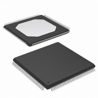
XCV50-6TQ144C Xilinx Inc, XCV50-6TQ144C Datasheet - Page 19

XCV50-6TQ144C
Manufacturer Part Number
XCV50-6TQ144C
Description
IC FPGA 2.5V C-TEMP 144-TQFP
Manufacturer
Xilinx Inc
Series
Virtex™r
Datasheet
1.XCV100-5PQ240C.pdf
(76 pages)
Specifications of XCV50-6TQ144C
Number Of Logic Elements/cells
1728
Number Of Labs/clbs
384
Total Ram Bits
32768
Number Of I /o
98
Number Of Gates
57906
Voltage - Supply
2.375 V ~ 2.625 V
Mounting Type
Surface Mount
Operating Temperature
0°C ~ 85°C
Package / Case
144-LQFP
Case
TQFP144
Dc
03+
Lead Free Status / RoHS Status
Contains lead / RoHS non-compliant
Available stocks
Company
Part Number
Manufacturer
Quantity
Price
Company:
Part Number:
XCV50-6TQ144C
Manufacturer:
XIL
Quantity:
1 238
Company:
Part Number:
XCV50-6TQ144C
Manufacturer:
XILINX
Quantity:
988
After configuration, the pins of the SelectMAP port can be
used as additional user I/O. Alternatively, the port can be
retained to permit high-speed 8-bit readback.
Retention of the SelectMAP port is selectable on a
design-by-design basis when the bitstream is generated. If
retention is selected, PROHIBIT constraints are required to
prevent the SelectMAP-port pins from being used as user
I/O.
Table 9: SelectMAP Write Timing Characteristics
Write
Write operations send packets of configuration data into the
FPGA. The sequence of operations for a multi-cycle write
operation is shown below. Note that a configuration packet
can be split into many such sequences. The packet does
not have to complete within one assertion of CS, illustrated
in
DS003-2 (v2.8.1) December 9, 2002
Product Specification
Figure
CCLK
16.
R
D
CS Setup/Hold
WRITE Setup/Hold
BUSY Propagation Delay
Maximum Frequency
Maximum Frequency with no handshake
0-7
Setup/Hold
FPGA checks data using CRC
FPGA enters start-up phase
and pulls INIT Low on error.
clearing pass and releases
causing DONE to go High.
Description
If no CRC errors found,
configuration memory.
FPGA starts to clear
FPGA makes a final
Once per bitstream,
INIT when finished.
Figure 15: Serial Configuration Flowchart
www.xilinx.com
1-800-255-7778
Configuration Completed
Load a Configuration Bit
Set PROGRAM = High
Multiple Virtex FPGAs can be configured using the Select-
MAP mode, and be made to start-up simultaneously. To
configure multiple devices in this way, wire the individual
CCLK, Data, WRITE, and BUSY pins of all the devices in
parallel. The individual devices are loaded separately by
asserting the CS pin of each device in turn and writing the
appropriate data.
Characteristics.
.
1. Assert WRITE and CS Low. Note that when CS is
2. Drive data onto D[7:0]. Note that to avoid contention,
1/2
3/4
5/6
7
Apply Power
Release INIT
Bitstream?
End of
asserted on successive CCLKs, WRITE must remain
either asserted or de-asserted. Otherwise an abort will
be initiated, as described below.
the data source should not be enabled while CS is Low
and WRITE is High. Similarly, while WRITE is High, no
more that one CS should be asserted.
INIT?
High
Yes
Virtex™ 2.5 V Field Programmable Gate Arrays
Low
T
T
T
SMCSCC
SMCCW
No
SMDCC
T
If used to delay
configuration
Symbol
F
SMCKBY
ds003_154_111799
S
F
CCNH
ee
CC
/T
/T
/T
SMCCD
SMCCCS
SMWCC
Table 9
for SelectMAP Write Timing
5.0 / 1.7
7.0 / 1.7
7.0 / 1.7
12.0
66
50
Module 2 of 4
MHz, max
MHz, max
ns, max
ns, min
ns, min
ns, min
Units
15


