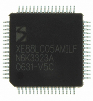
XE8805AMI028LF Semtech, XE8805AMI028LF Datasheet - Page 98

XE8805AMI028LF
Manufacturer Part Number
XE8805AMI028LF
Description
IC DAS 16BIT FLASH 8K MTP 64LQFP
Manufacturer
Semtech
Datasheet
1.XE8805AMI028LF.pdf
(156 pages)
Specifications of XE8805AMI028LF
Applications
Sensing Machine
Core Processor
RISC
Program Memory Type
FLASH (22 kB)
Controller Series
XE8000
Ram Size
512 x 8
Interface
UART, USRT
Number Of I /o
24
Voltage - Supply
2.4 V ~ 5.5 V
Operating Temperature
-40°C ~ 85°C
Mounting Type
Surface Mount
Package / Case
64-LQFP
Supply Voltage Range
2.4V To 5.5V
Operating Temperature Range
-40°C To +85°C
Digital Ic Case Style
LQFP
No. Of Pins
64
For Use With
XE8000MP - PROG BOARD AND PROSTART2 CARD
Lead Free Status / RoHS Status
Lead free / RoHS Compliant
Available stocks
Company
Part Number
Manufacturer
Quantity
Price
Part Number:
XE8805AMI028LF
Manufacturer:
SEMTECH/美国升特
Quantity:
20 000
16.6.1
Depending on the application objectives, the user may enable or bypass each PGA stage. This is done according to
the word ENABLE and the coding given in Table 16-13. To reduce power dissipation, the ADC can also be
inactivated while idle.
16.6.2
The first stage can have a buffer function (unity gain) or provide a gain of 10 (see Table 16-14). The voltage V
the output of PGA1 is:
where GD
16.6.3
The second PGA has a finer gain and offset tuning capability, as shown in Table 16-15 and Table 16-16. The
voltage V
where GD
PGA2_GAIN[1:0] and PGA2_OFFSET[3:0].
As shown in equation 6, the offset correction is directly proportional to the reference voltage. All drifts and
perturbations on the reference voltage will affect the precision of the offset compensation.
16.6.4
The finest gain and offset tuning is performed with the third and last PGA stage, according to the coding of Table
16-17 and Table 16-18. The output of PGA3 is also the input of the ADC. Thus, similarly to PGA2, we find that the
voltage entering the ADC is given by:
where GD
PGA3_GAIN[6:0] and PGA3_OFFSET[6:0] . To remain within the signal compliance of the PGA stages, the
condition:
must be verified.
As shown in equation 7, the offset correction is directly proportional to the reference voltage. All drifts and
perturbations on the reference voltage will affect the precision of the offset compensation.
© Semtech 2006
V
V
V
V
D2
D
D
IN
D
1
2
1
1
2
PGA & ADC Enabling
PGA1
PGA2
PGA3
,
3
is the gain of PGA1 (in V/V) controlled with the bit PGA1_GAIN.
,
ADC
at the output of PGA2 is given by:
and GDoff
=
=
V
and GDoff
D
GD
GD
2
=
<
1
GD
2
V
⋅
⋅
V
V
DD
IN
3
D
⋅
1
2
V
−
D
are respectively the gain and offset of PGA2 (in V/V). These are controlled with the words
(V)
GDoff
3
2
−
are respectively the gain and offset of PGA3 (in V/V). The control words are
GDoff
2
(V)
⋅
V
3
REF
⋅
V
REF
(V)
(V)
16-12
(Eq. 5)
(Eq. 6)
(Eq. 7)
(Eq. 8)
XE8805/05A
www.semtech.com
D1
at


