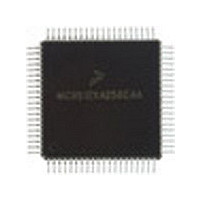
MC9S12C128VFU Freescale Semiconductor, MC9S12C128VFU Datasheet - Page 122

MC9S12C128VFU
Manufacturer Part Number
MC9S12C128VFU
Description
Manufacturer
Freescale Semiconductor
Datasheet
1.MC9S12C128VFU.pdf
(690 pages)
Specifications of MC9S12C128VFU
Cpu Family
HCS12
Device Core Size
16b
Frequency (max)
25MHz
Interface Type
CAN/SCI/SPI
Program Memory Type
Flash
Program Memory Size
128KB
Total Internal Ram Size
4KB
# I/os (max)
60
Number Of Timers - General Purpose
8
Operating Supply Voltage (typ)
2.5/5V
Operating Supply Voltage (max)
2.75/5.5V
Operating Supply Voltage (min)
2.35/2.97V
On-chip Adc
8-chx10-bit
Instruction Set Architecture
CISC
Operating Temp Range
-40C to 105C
Operating Temperature Classification
Industrial
Mounting
Surface Mount
Pin Count
80
Package Type
PQFP
Lead Free Status / Rohs Status
Not Compliant
Available stocks
Company
Part Number
Manufacturer
Quantity
Price
Company:
Part Number:
MC9S12C128VFUE
Manufacturer:
Freescale
Quantity:
38 000
Company:
Part Number:
MC9S12C128VFUE
Manufacturer:
Freescale Semiconductor
Quantity:
10 000
- Current page: 122 of 690
- Download datasheet (4Mb)
Chapter 3 Module Mapping Control (MMCV4) Block Description
3.4
The MMC sub-block performs four basic functions of the core operation: bus control, address decoding
and select signal generation, memory expansion, and security decoding for the system. Each aspect is
described in the following subsections.
3.4.1
The MMC controls the address bus and data buses that interface the core with the rest of the system. This
includes the multiplexing of the input data buses to the core onto the main CPU read data bus and control
of data flow from the CPU to the output address and data buses of the core. In addition, the MMC manages
all CPU read data bus swapping operations.
3.4.2
As data flows on the core address bus, the MMC decodes the address information, determines whether the
internal core register or firmware space, the peripheral space or a memory register or array space is being
addressed and generates the correct select signal. This decoding operation also interprets the mode of
operation of the system and the state of the mapping control registers in order to generate the proper select.
The MMC also generates two external chip select signals, emulation chip select (ECS) and external chip
select (XCS).
3.4.2.1
Although internal resources such as control registers and on-chip memory have default addresses, each can
be relocated by changing the default values in control registers. Normally, I/O addresses, control registers,
122
Functional Description
Bus Control
Address Decoding
Select Priority and Mode Considerations
PIX5
0
0
0
0
1
1
1
1
.
.
.
.
.
PIX4
0
0
0
0
1
1
1
1
.
.
.
.
.
Table 3-14. Program Page Index Register Bits
PIX3
MC9S12C-Family / MC9S12GC-Family
0
0
0
0
1
1
1
1
.
.
.
.
PIX2
0
0
0
0
1
1
1
1
.
.
.
.
.
Rev 01.24
PIX1
0
0
1
1
0
0
1
1
.
.
.
.
.
PIX0
0
1
0
1
0
1
0
1
.
.
.
.
.
Program Space
16K page 60
16K page 61
16K page 62
16K page 63
16K page 0
16K page 1
16K page 2
16K page 3
Selected
.
.
.
.
.
Freescale Semiconductor
Related parts for MC9S12C128VFU
Image
Part Number
Description
Manufacturer
Datasheet
Request
R
Part Number:
Description:
Manufacturer:
Freescale Semiconductor, Inc
Datasheet:
Part Number:
Description:
Manufacturer:
Freescale Semiconductor, Inc
Datasheet:
Part Number:
Description:
Manufacturer:
Freescale Semiconductor, Inc
Datasheet:
Part Number:
Description:
Manufacturer:
Freescale Semiconductor, Inc
Datasheet:
Part Number:
Description:
Manufacturer:
Freescale Semiconductor, Inc
Datasheet:
Part Number:
Description:
Manufacturer:
Freescale Semiconductor, Inc
Datasheet:
Part Number:
Description:
Manufacturer:
Freescale Semiconductor, Inc
Datasheet:
Part Number:
Description:
Manufacturer:
Freescale Semiconductor, Inc
Datasheet:
Part Number:
Description:
Manufacturer:
Freescale Semiconductor, Inc
Datasheet:
Part Number:
Description:
Manufacturer:
Freescale Semiconductor, Inc
Datasheet:
Part Number:
Description:
Manufacturer:
Freescale Semiconductor, Inc
Datasheet:
Part Number:
Description:
Manufacturer:
Freescale Semiconductor, Inc
Datasheet:
Part Number:
Description:
Manufacturer:
Freescale Semiconductor, Inc
Datasheet:
Part Number:
Description:
Manufacturer:
Freescale Semiconductor, Inc
Datasheet:
Part Number:
Description:
Manufacturer:
Freescale Semiconductor, Inc
Datasheet:


