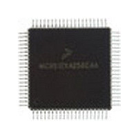
MC9S12C128VFU Freescale Semiconductor, MC9S12C128VFU Datasheet - Page 430

MC9S12C128VFU
Manufacturer Part Number
MC9S12C128VFU
Description
Manufacturer
Freescale Semiconductor
Datasheet
1.MC9S12C128VFU.pdf
(690 pages)
Specifications of MC9S12C128VFU
Cpu Family
HCS12
Device Core Size
16b
Frequency (max)
25MHz
Interface Type
CAN/SCI/SPI
Program Memory Type
Flash
Program Memory Size
128KB
Total Internal Ram Size
4KB
# I/os (max)
60
Number Of Timers - General Purpose
8
Operating Supply Voltage (typ)
2.5/5V
Operating Supply Voltage (max)
2.75/5.5V
Operating Supply Voltage (min)
2.35/2.97V
On-chip Adc
8-chx10-bit
Instruction Set Architecture
CISC
Operating Temp Range
-40C to 105C
Operating Temperature Classification
Industrial
Mounting
Surface Mount
Pin Count
80
Package Type
PQFP
Lead Free Status / Rohs Status
Not Compliant
Available stocks
Company
Part Number
Manufacturer
Quantity
Price
Company:
Part Number:
MC9S12C128VFUE
Manufacturer:
Freescale
Quantity:
38 000
Company:
Part Number:
MC9S12C128VFUE
Manufacturer:
Freescale Semiconductor
Quantity:
10 000
- Current page: 430 of 690
- Download datasheet (4Mb)
Chapter 14 Serial Peripheral Interface (SPIV3) Block Description
The baud rate generator is activated only when the SPI is in the master mode and a serial transfer is taking
place. In the other cases, the divider is disabled to decrease I
14.4.5
14.4.5.1
The SS output feature automatically drives the SS pin low during transmission to select external devices
and drives it high during idle to deselect external devices. When SS output is selected, the SS output pin
is connected to the SS input pin of the external device.
The SS output is available only in master mode during normal SPI operation by asserting SSOE and
MODFEN bit as shown in
The mode fault feature is disabled while SS output is enabled.
14.4.5.2
The bidirectional mode is selected when the SPC0 bit is set in SPI Control Register 2 (see
this mode, the SPI uses only one serial data pin for the interface with external device(s). The MSTR bit
decides which pin to use. The MOSI pin becomes the serial data I/O (MOMI) pin for the master mode, and
the MISO pin becomes serial data I/O (SISO) pin for the slave mode. The MISO pin in master mode and
MOSI pin in slave mode are not used by the SPI.
430
Bidirectional Mode
When SPE = 1
Normal Mode
SPC0 = 0
SPC0 = 1
Special Features
SS Output
Bidirectional Mode (MOSI or MISO)
Care must be taken when using the SS output feature in a multimaster
system because the mode fault feature is not available for detecting system
errors between masters.
Serial Out
Serial Out
Table
Serial In
Serial In
Table 14-9. Normal Mode and Bidirectional Mode
SPI
SPI
BaudRateDivisor
Figure 14-11. Baud Rate Divisor Equation
Master Mode MSTR = 1
14-3.
MC9S12C-Family / MC9S12GC-Family
BIDIROE
Rev 01.24
=
NOTE
(
SPPR
MOMI
MOSI
MISO
+
1
DD
) 2
•
current.
(
SPR
Serial Out
Serial Out
+
Serial In
Serial In
SPI
SPI
1
)
Slave Mode MSTR = 0
BIDIROE
Freescale Semiconductor
Table
MOSI
MISO
SISO
14-9). In
Related parts for MC9S12C128VFU
Image
Part Number
Description
Manufacturer
Datasheet
Request
R
Part Number:
Description:
Manufacturer:
Freescale Semiconductor, Inc
Datasheet:
Part Number:
Description:
Manufacturer:
Freescale Semiconductor, Inc
Datasheet:
Part Number:
Description:
Manufacturer:
Freescale Semiconductor, Inc
Datasheet:
Part Number:
Description:
Manufacturer:
Freescale Semiconductor, Inc
Datasheet:
Part Number:
Description:
Manufacturer:
Freescale Semiconductor, Inc
Datasheet:
Part Number:
Description:
Manufacturer:
Freescale Semiconductor, Inc
Datasheet:
Part Number:
Description:
Manufacturer:
Freescale Semiconductor, Inc
Datasheet:
Part Number:
Description:
Manufacturer:
Freescale Semiconductor, Inc
Datasheet:
Part Number:
Description:
Manufacturer:
Freescale Semiconductor, Inc
Datasheet:
Part Number:
Description:
Manufacturer:
Freescale Semiconductor, Inc
Datasheet:
Part Number:
Description:
Manufacturer:
Freescale Semiconductor, Inc
Datasheet:
Part Number:
Description:
Manufacturer:
Freescale Semiconductor, Inc
Datasheet:
Part Number:
Description:
Manufacturer:
Freescale Semiconductor, Inc
Datasheet:
Part Number:
Description:
Manufacturer:
Freescale Semiconductor, Inc
Datasheet:
Part Number:
Description:
Manufacturer:
Freescale Semiconductor, Inc
Datasheet:


