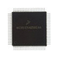
MC9S12C128VFU Freescale Semiconductor, MC9S12C128VFU Datasheet - Page 76

MC9S12C128VFU
Manufacturer Part Number
MC9S12C128VFU
Description
Manufacturer
Freescale Semiconductor
Datasheet
1.MC9S12C128VFU.pdf
(690 pages)
Specifications of MC9S12C128VFU
Cpu Family
HCS12
Device Core Size
16b
Frequency (max)
25MHz
Interface Type
CAN/SCI/SPI
Program Memory Type
Flash
Program Memory Size
128KB
Total Internal Ram Size
4KB
# I/os (max)
60
Number Of Timers - General Purpose
8
Operating Supply Voltage (typ)
2.5/5V
Operating Supply Voltage (max)
2.75/5.5V
Operating Supply Voltage (min)
2.35/2.97V
On-chip Adc
8-chx10-bit
Instruction Set Architecture
CISC
Operating Temp Range
-40C to 105C
Operating Temperature Classification
Industrial
Mounting
Surface Mount
Pin Count
80
Package Type
PQFP
Lead Free Status / Rohs Status
Not Compliant
Available stocks
Company
Part Number
Manufacturer
Quantity
Price
Company:
Part Number:
MC9S12C128VFUE
Manufacturer:
Freescale
Quantity:
38 000
Company:
Part Number:
MC9S12C128VFUE
Manufacturer:
Freescale Semiconductor
Quantity:
10 000
- Current page: 76 of 690
- Download datasheet (4Mb)
Chapter 2 Port Integration Module (PIM9C32) Block Description
2.2
This section lists and describes the signals that do connect off-chip.
Table 2-1
one function associated to a pin, the priority is indicated by the position in the table from top (highest
priority) to down (lowest priority).
76
Port AD
Port M
Port S
Port P
Port A
Port B
Port T
Port J
Port
Signal Description
Pin Name
shows all pins and their functions that are controlled by the PIM module. If there is more than
PAD[7:0]
PT[7:0]
PP[7:0]
PB[7:0]
PJ[7:6]
PA[7:0]
PP[6]
PM5
PM4
PM3
PM2
PM1
PM0
PS3
PS2
PS1
PS0
Pin Function
ADDR[15:8]/
DATA[15:8]/
ADDR[7:0]/
DATA[7:0]/
PWM[4:0]
PWM[5:0]
GPIO[7:0]
GPIO[7:0]
ROMON
ATD[7:0]
IOC[7:0]
RXCAN
TXCAN
GPIO
GPIO
GPIO
GPIO
GPIO
MOSI
MISO
GPIO
GPIO
GPIO
RXD
TXD
SCK
SS
Table 2-1. Pin Functions and Priorities
MC9S12C-Family / MC9S12GC-Family
PWM outputs (only available if enabled in MODRR register)
Standard timer channels
General-purpose I/O
General-purpose I/O
General purpose I/O
Serial communication interface transmit pin
General-purpose I/O
Serial communication interface receive pin
General-purpose I/O
SPI clock
SPI transmit pin
SPI slave select line
SPI receive pin
MSCAN transmit pin
MSCAN receive pin
PWM outputs
General purpose I/O with interrupt
ROMON input signal
General purpose I/O with interrupt
ATD analog inputs
General purpose I/O
Refer to MEBI Block Guide.
Refer to MEBI Block Guide.
Rev 01.24
Description
Freescale Semiconductor
Pin Function
after Reset
GPIO
Related parts for MC9S12C128VFU
Image
Part Number
Description
Manufacturer
Datasheet
Request
R
Part Number:
Description:
Manufacturer:
Freescale Semiconductor, Inc
Datasheet:
Part Number:
Description:
Manufacturer:
Freescale Semiconductor, Inc
Datasheet:
Part Number:
Description:
Manufacturer:
Freescale Semiconductor, Inc
Datasheet:
Part Number:
Description:
Manufacturer:
Freescale Semiconductor, Inc
Datasheet:
Part Number:
Description:
Manufacturer:
Freescale Semiconductor, Inc
Datasheet:
Part Number:
Description:
Manufacturer:
Freescale Semiconductor, Inc
Datasheet:
Part Number:
Description:
Manufacturer:
Freescale Semiconductor, Inc
Datasheet:
Part Number:
Description:
Manufacturer:
Freescale Semiconductor, Inc
Datasheet:
Part Number:
Description:
Manufacturer:
Freescale Semiconductor, Inc
Datasheet:
Part Number:
Description:
Manufacturer:
Freescale Semiconductor, Inc
Datasheet:
Part Number:
Description:
Manufacturer:
Freescale Semiconductor, Inc
Datasheet:
Part Number:
Description:
Manufacturer:
Freescale Semiconductor, Inc
Datasheet:
Part Number:
Description:
Manufacturer:
Freescale Semiconductor, Inc
Datasheet:
Part Number:
Description:
Manufacturer:
Freescale Semiconductor, Inc
Datasheet:
Part Number:
Description:
Manufacturer:
Freescale Semiconductor, Inc
Datasheet:


