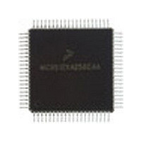
MC9S12C128VFU Freescale Semiconductor, MC9S12C128VFU Datasheet - Page 243

MC9S12C128VFU
Manufacturer Part Number
MC9S12C128VFU
Description
Manufacturer
Freescale Semiconductor
Datasheet
1.MC9S12C128VFU.pdf
(690 pages)
Specifications of MC9S12C128VFU
Cpu Family
HCS12
Device Core Size
16b
Frequency (max)
25MHz
Interface Type
CAN/SCI/SPI
Program Memory Type
Flash
Program Memory Size
128KB
Total Internal Ram Size
4KB
# I/os (max)
60
Number Of Timers - General Purpose
8
Operating Supply Voltage (typ)
2.5/5V
Operating Supply Voltage (max)
2.75/5.5V
Operating Supply Voltage (min)
2.35/2.97V
On-chip Adc
8-chx10-bit
Instruction Set Architecture
CISC
Operating Temp Range
-40C to 105C
Operating Temperature Classification
Industrial
Mounting
Surface Mount
Pin Count
80
Package Type
PQFP
Lead Free Status / Rohs Status
Not Compliant
Available stocks
Company
Part Number
Manufacturer
Quantity
Price
Company:
Part Number:
MC9S12C128VFUE
Manufacturer:
Freescale
Quantity:
38 000
Company:
Part Number:
MC9S12C128VFUE
Manufacturer:
Freescale Semiconductor
Quantity:
10 000
- Current page: 243 of 690
- Download datasheet (4Mb)
8.3.2.12
The data port associated with the ATD is general purpose I/O. The port pins are shared with the analog
A/D inputs AN7–AN0.
Read: Anytime
Write: Anytime, no effect
The A/D input channels may be used for general-purpose digital I/0.
8.3.2.13
The A/D conversion results are stored in 8 read-only result registers ATDDRHx/ATDDRLx. The result
data is formatted in the result registers based on two criteria. First there is left and right justification; this
selection is made using the DJM control bit in ATDCTL5. Second there is signed and unsigned data; this
selection is made using the DSGN control bit in ATDCTL5. Signed data is stored in 2’s complement
format and only exists in left justified format. Signed data selected for right justified format is ignored.
Read: Anytime
Write: Anytime, no effect in normal modes
Freescale Semiconductor
Function
Module Base + 0x000F
PTAD[7:0]
Reset
Field
Pin
7
W
R
PTAD7
AN7
A/D Channel x (ANx) Digital Input (x = 7, 6, 5, 4, 3, 2, 1, 0) — If the digital input buffer on the ANx pin is enabled
(IENx = 1) read returns the logic level on ANx pin (signal potentials not meeting V
an indeterminate value)).
If the digital input buffers are disabled (IENx = 0), read returns a “1”.
Reset sets all PORTAD bits to “1”.
Port Data Register (PORTAD)
ATD Conversion Result Registers (ATDDRHx/ATDDRLx)
1
7
= Unimplemented or Reserved
PTAD6
AN6
1
6
Figure 8-14. Port Data Register (PORTAD)
Table 8-18. PORTAD Field Descriptions
PTAD5
MC9S12C-Family / MC9S12GC-Family
AN5
1
5
PTAD4
Rev 01.24
AN4
1
4
Chapter 8 Analog-to-Digital Converter (ATD10B8C) Block Description
Description
PTAD3
AN3‘
1
3
PTAD2
AN2
1
2
IL
or V
IH
PTAD1
AN1
specifications will have
1
1
PTAD0
AN0
1
0
243
Related parts for MC9S12C128VFU
Image
Part Number
Description
Manufacturer
Datasheet
Request
R
Part Number:
Description:
Manufacturer:
Freescale Semiconductor, Inc
Datasheet:
Part Number:
Description:
Manufacturer:
Freescale Semiconductor, Inc
Datasheet:
Part Number:
Description:
Manufacturer:
Freescale Semiconductor, Inc
Datasheet:
Part Number:
Description:
Manufacturer:
Freescale Semiconductor, Inc
Datasheet:
Part Number:
Description:
Manufacturer:
Freescale Semiconductor, Inc
Datasheet:
Part Number:
Description:
Manufacturer:
Freescale Semiconductor, Inc
Datasheet:
Part Number:
Description:
Manufacturer:
Freescale Semiconductor, Inc
Datasheet:
Part Number:
Description:
Manufacturer:
Freescale Semiconductor, Inc
Datasheet:
Part Number:
Description:
Manufacturer:
Freescale Semiconductor, Inc
Datasheet:
Part Number:
Description:
Manufacturer:
Freescale Semiconductor, Inc
Datasheet:
Part Number:
Description:
Manufacturer:
Freescale Semiconductor, Inc
Datasheet:
Part Number:
Description:
Manufacturer:
Freescale Semiconductor, Inc
Datasheet:
Part Number:
Description:
Manufacturer:
Freescale Semiconductor, Inc
Datasheet:
Part Number:
Description:
Manufacturer:
Freescale Semiconductor, Inc
Datasheet:
Part Number:
Description:
Manufacturer:
Freescale Semiconductor, Inc
Datasheet:


