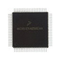
MC9S12C128VFU Freescale Semiconductor, MC9S12C128VFU Datasheet - Page 86

MC9S12C128VFU
Manufacturer Part Number
MC9S12C128VFU
Description
Manufacturer
Freescale Semiconductor
Datasheet
1.MC9S12C128VFU.pdf
(690 pages)
Specifications of MC9S12C128VFU
Cpu Family
HCS12
Device Core Size
16b
Frequency (max)
25MHz
Interface Type
CAN/SCI/SPI
Program Memory Type
Flash
Program Memory Size
128KB
Total Internal Ram Size
4KB
# I/os (max)
60
Number Of Timers - General Purpose
8
Operating Supply Voltage (typ)
2.5/5V
Operating Supply Voltage (max)
2.75/5.5V
Operating Supply Voltage (min)
2.35/2.97V
On-chip Adc
8-chx10-bit
Instruction Set Architecture
CISC
Operating Temp Range
-40C to 105C
Operating Temperature Classification
Industrial
Mounting
Surface Mount
Pin Count
80
Package Type
PQFP
Lead Free Status / Rohs Status
Not Compliant
Available stocks
Company
Part Number
Manufacturer
Quantity
Price
Company:
Part Number:
MC9S12C128VFUE
Manufacturer:
Freescale
Quantity:
38 000
Company:
Part Number:
MC9S12C128VFUE
Manufacturer:
Freescale Semiconductor
Quantity:
10 000
- Current page: 86 of 690
- Download datasheet (4Mb)
Chapter 2 Port Integration Module (PIM9C32) Block Description
2.3.2.2.3
Read: Anytime.
Write: Anytime.
86
Module Base + 0x000A
DDRS[3:0]
Reset
Field
3–0
W
R
Direction Register Port S — This register configures each port S pin as either input or output.
If the associated SCI transmit or receive channel is enabled this register has no effect on the pins. The pin is
forced to be an output if the SCI transmit channel is enabled, it is forced to be an input if the SCI receive channel
is enabled.
The DDRS bits revert to controlling the I/O direction of a pin when the associated channel is disabled.
0 Associated pin is configured as input.
1 Associated pin is configured as output.
Note: Due to internal synchronization circuits, it can take up to 2 bus cycles until the correct value is read on PTS
0
0
7
Port S Data Direction Register (DDRS)
or PTIS registers, when changing the DDRS register.
= Unimplemented or Reserved
0
0
6
Figure 2-12. Port S Data Direction Register (DDRS)
Table 2-11. DDRS Field Descriptions
MC9S12C-Family / MC9S12GC-Family
0
0
5
Rev 01.24
0
0
4
Description
DDRS3
0
3
DDRS2
0
2
DDRS1
Freescale Semiconductor
0
1
DDRS0
0
0
Related parts for MC9S12C128VFU
Image
Part Number
Description
Manufacturer
Datasheet
Request
R
Part Number:
Description:
Manufacturer:
Freescale Semiconductor, Inc
Datasheet:
Part Number:
Description:
Manufacturer:
Freescale Semiconductor, Inc
Datasheet:
Part Number:
Description:
Manufacturer:
Freescale Semiconductor, Inc
Datasheet:
Part Number:
Description:
Manufacturer:
Freescale Semiconductor, Inc
Datasheet:
Part Number:
Description:
Manufacturer:
Freescale Semiconductor, Inc
Datasheet:
Part Number:
Description:
Manufacturer:
Freescale Semiconductor, Inc
Datasheet:
Part Number:
Description:
Manufacturer:
Freescale Semiconductor, Inc
Datasheet:
Part Number:
Description:
Manufacturer:
Freescale Semiconductor, Inc
Datasheet:
Part Number:
Description:
Manufacturer:
Freescale Semiconductor, Inc
Datasheet:
Part Number:
Description:
Manufacturer:
Freescale Semiconductor, Inc
Datasheet:
Part Number:
Description:
Manufacturer:
Freescale Semiconductor, Inc
Datasheet:
Part Number:
Description:
Manufacturer:
Freescale Semiconductor, Inc
Datasheet:
Part Number:
Description:
Manufacturer:
Freescale Semiconductor, Inc
Datasheet:
Part Number:
Description:
Manufacturer:
Freescale Semiconductor, Inc
Datasheet:
Part Number:
Description:
Manufacturer:
Freescale Semiconductor, Inc
Datasheet:


