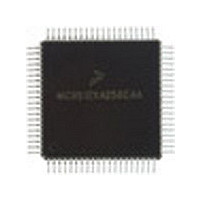
MC9S12C128VFU Freescale Semiconductor, MC9S12C128VFU Datasheet - Page 409

MC9S12C128VFU
Manufacturer Part Number
MC9S12C128VFU
Description
Manufacturer
Freescale Semiconductor
Datasheet
1.MC9S12C128VFU.pdf
(690 pages)
Specifications of MC9S12C128VFU
Cpu Family
HCS12
Device Core Size
16b
Frequency (max)
25MHz
Interface Type
CAN/SCI/SPI
Program Memory Type
Flash
Program Memory Size
128KB
Total Internal Ram Size
4KB
# I/os (max)
60
Number Of Timers - General Purpose
8
Operating Supply Voltage (typ)
2.5/5V
Operating Supply Voltage (max)
2.75/5.5V
Operating Supply Voltage (min)
2.35/2.97V
On-chip Adc
8-chx10-bit
Instruction Set Architecture
CISC
Operating Temp Range
-40C to 105C
Operating Temperature Classification
Industrial
Mounting
Surface Mount
Pin Count
80
Package Type
PQFP
Lead Free Status / Rohs Status
Not Compliant
Available stocks
Company
Part Number
Manufacturer
Quantity
Price
Company:
Part Number:
MC9S12C128VFUE
Manufacturer:
Freescale
Quantity:
38 000
Company:
Part Number:
MC9S12C128VFUE
Manufacturer:
Freescale Semiconductor
Quantity:
10 000
- Current page: 409 of 690
- Download datasheet (4Mb)
13.4.5
Normally, the SCI uses two pins for transmitting and receiving. In single-wire operation, the RXD pin is
disconnected from the SCI. The SCI uses the TXD pin for both receiving and transmitting.
Enable single-wire operation by setting the LOOPS bit and the receiver source bit, RSRC, in SCI control
register 1 (SCICR1). Setting the LOOPS bit disables the path from the Rx Input signal to the receiver.
Setting the RSRC bit connects the receiver input to the output of the TXD pin driver. Both the transmitter
and receiver must be enabled (TE = 1 and RE = 1).The TXDIR bit (SCISR2[1]) determines whether the
TXD pin is going to be used as an input (TXDIR = 0) or an output (TXDIR = 1) in this mode of operation.
13.4.6
In loop operation the transmitter output goes to the receiver input. The Rx Input signal is disconnected
from the SCI
Enable loop operation by setting the LOOPS bit and clearing the RSRC bit in SCI control register 1
(SCICR1). Setting the LOOPS bit disables the path from the Rx Input signal to the receiver. Clearing the
RSRC bit connects the transmitter output to the receiver input. Both the transmitter and receiver must be
enabled (TE = 1 and RE = 1).
13.5
13.5.1
The reset state of each individual bit is listed in
the registers and their bit fields. All special functions or modes which are initialized during or just
following reset are described within this section.
Freescale Semiconductor
.
Initialization Information
Single-Wire Operation
Loop Operation
Reset Initialization
Figure 13-22. Single-Wire Operation (LOOPS = 1, RSRC = 1)
Figure 13-23. Loop Operation (LOOPS = 1, RSRC = 0)
TRANSMITTER
TRANSMITTER
RECEIVER
RECEIVER
MC9S12C-Family / MC9S12GC-Family
Chapter 13 Serial Communications Interface (S12SCIV2) Block Description
Section 13.3, “Memory Map and Registers”
Rev 01.24
Tx OUTPUT SIGNAL
Tx OUTPUT SIGNAL
Tx INPUT SIGNAL
RXD
RXD
which details
409
Related parts for MC9S12C128VFU
Image
Part Number
Description
Manufacturer
Datasheet
Request
R
Part Number:
Description:
Manufacturer:
Freescale Semiconductor, Inc
Datasheet:
Part Number:
Description:
Manufacturer:
Freescale Semiconductor, Inc
Datasheet:
Part Number:
Description:
Manufacturer:
Freescale Semiconductor, Inc
Datasheet:
Part Number:
Description:
Manufacturer:
Freescale Semiconductor, Inc
Datasheet:
Part Number:
Description:
Manufacturer:
Freescale Semiconductor, Inc
Datasheet:
Part Number:
Description:
Manufacturer:
Freescale Semiconductor, Inc
Datasheet:
Part Number:
Description:
Manufacturer:
Freescale Semiconductor, Inc
Datasheet:
Part Number:
Description:
Manufacturer:
Freescale Semiconductor, Inc
Datasheet:
Part Number:
Description:
Manufacturer:
Freescale Semiconductor, Inc
Datasheet:
Part Number:
Description:
Manufacturer:
Freescale Semiconductor, Inc
Datasheet:
Part Number:
Description:
Manufacturer:
Freescale Semiconductor, Inc
Datasheet:
Part Number:
Description:
Manufacturer:
Freescale Semiconductor, Inc
Datasheet:
Part Number:
Description:
Manufacturer:
Freescale Semiconductor, Inc
Datasheet:
Part Number:
Description:
Manufacturer:
Freescale Semiconductor, Inc
Datasheet:
Part Number:
Description:
Manufacturer:
Freescale Semiconductor, Inc
Datasheet:


