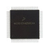
MC9S12C128VFU Freescale Semiconductor, MC9S12C128VFU Datasheet - Page 465

MC9S12C128VFU
Manufacturer Part Number
MC9S12C128VFU
Description
Manufacturer
Freescale Semiconductor
Datasheet
1.MC9S12C128VFU.pdf
(690 pages)
Specifications of MC9S12C128VFU
Cpu Family
HCS12
Device Core Size
16b
Frequency (max)
25MHz
Interface Type
CAN/SCI/SPI
Program Memory Type
Flash
Program Memory Size
128KB
Total Internal Ram Size
4KB
# I/os (max)
60
Number Of Timers - General Purpose
8
Operating Supply Voltage (typ)
2.5/5V
Operating Supply Voltage (max)
2.75/5.5V
Operating Supply Voltage (min)
2.35/2.97V
On-chip Adc
8-chx10-bit
Instruction Set Architecture
CISC
Operating Temp Range
-40C to 105C
Operating Temperature Classification
Industrial
Mounting
Surface Mount
Pin Count
80
Package Type
PQFP
Lead Free Status / Rohs Status
Not Compliant
Available stocks
Company
Part Number
Manufacturer
Quantity
Price
Company:
Part Number:
MC9S12C128VFUE
Manufacturer:
Freescale
Quantity:
38 000
Company:
Part Number:
MC9S12C128VFUE
Manufacturer:
Freescale Semiconductor
Quantity:
10 000
- Current page: 465 of 690
- Download datasheet (4Mb)
16.2
Due to the nature of VREG3V3V2 being a voltage regulator providing the chip internal power supply
voltages most signals are power supply signals connected to pads.
Table 16-1
16.2.1
Signal V
through this pin. A chip external decoupling capacitor (100 nF...220 nF, X7R ceramic) between V
V
For entering Shutdown Mode, pin V
16.2.2
Signals V
regulator. Internal precision reference circuits are supplied from these signals. A chip external decoupling
capacitor (100 nF...220 nF, X7R ceramic) between V
supply.
Freescale Semiconductor
SSR
V
REGEN
can smoothen ripple on V
V
V
Name
DDR
V
V
V
DDPLL
V
SSPLL
External Signal Description
V
DDA
DDR
DDA
SSA
DD
SS
(optional)
shows all signals of VREG3V3V2 associated with pins.
V
V
is the power input of VREG3V3V2. All currents sourced into the regulator loads flow
DDR
DDA
/V
Check device overview chapter for connectivity of the signals.
SSA
, V
— Regulator Power Input
which are supposed to be relatively quiet are used to supply the analog parts of the
SSA
Port
—
—
—
—
—
—
—
—
— Regulator Reference Supply
Table 16-1. VREG3V3V2 — Signal Properties
DDR
VREG3V3V2 power input (positive supply)
VREG3V3V2 quiet input (positive supply)
VREG3V3V2 quiet input (ground)
VREG3V3V2 primary output (positive supply)
VREG3V3V2 primary output (ground)
VREG3V3V2 secondary output (positive supply)
VREG3V3V2 secondary output (ground)
VREG3V3V2 (Optional) Regulator Enable
.
DDR
MC9S12C-Family / MC9S12GC-Family
should also be tied to ground on devices without a V
Chapter 16 Dual Output Voltage Regulator (VREG3V3V2) Block Description
Rev 01.24
NOTE
Function
DDA
and V
SSA
can further improve the quality of this
Reset State
—
—
—
—
—
—
—
—
REGEN
DDR
Pull Up
—
—
—
—
—
—
—
—
and
pin.
465
Related parts for MC9S12C128VFU
Image
Part Number
Description
Manufacturer
Datasheet
Request
R
Part Number:
Description:
Manufacturer:
Freescale Semiconductor, Inc
Datasheet:
Part Number:
Description:
Manufacturer:
Freescale Semiconductor, Inc
Datasheet:
Part Number:
Description:
Manufacturer:
Freescale Semiconductor, Inc
Datasheet:
Part Number:
Description:
Manufacturer:
Freescale Semiconductor, Inc
Datasheet:
Part Number:
Description:
Manufacturer:
Freescale Semiconductor, Inc
Datasheet:
Part Number:
Description:
Manufacturer:
Freescale Semiconductor, Inc
Datasheet:
Part Number:
Description:
Manufacturer:
Freescale Semiconductor, Inc
Datasheet:
Part Number:
Description:
Manufacturer:
Freescale Semiconductor, Inc
Datasheet:
Part Number:
Description:
Manufacturer:
Freescale Semiconductor, Inc
Datasheet:
Part Number:
Description:
Manufacturer:
Freescale Semiconductor, Inc
Datasheet:
Part Number:
Description:
Manufacturer:
Freescale Semiconductor, Inc
Datasheet:
Part Number:
Description:
Manufacturer:
Freescale Semiconductor, Inc
Datasheet:
Part Number:
Description:
Manufacturer:
Freescale Semiconductor, Inc
Datasheet:
Part Number:
Description:
Manufacturer:
Freescale Semiconductor, Inc
Datasheet:
Part Number:
Description:
Manufacturer:
Freescale Semiconductor, Inc
Datasheet:


