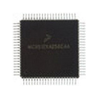
MC9S12C128VFU Freescale Semiconductor, MC9S12C128VFU Datasheet - Page 55

MC9S12C128VFU
Manufacturer Part Number
MC9S12C128VFU
Description
Manufacturer
Freescale Semiconductor
Datasheet
1.MC9S12C128VFU.pdf
(690 pages)
Specifications of MC9S12C128VFU
Cpu Family
HCS12
Device Core Size
16b
Frequency (max)
25MHz
Interface Type
CAN/SCI/SPI
Program Memory Type
Flash
Program Memory Size
128KB
Total Internal Ram Size
4KB
# I/os (max)
60
Number Of Timers - General Purpose
8
Operating Supply Voltage (typ)
2.5/5V
Operating Supply Voltage (max)
2.75/5.5V
Operating Supply Voltage (min)
2.35/2.97V
On-chip Adc
8-chx10-bit
Instruction Set Architecture
CISC
Operating Temp Range
-40C to 105C
Operating Temperature Classification
Industrial
Mounting
Surface Mount
Pin Count
80
Package Type
PQFP
Lead Free Status / Rohs Status
Not Compliant
Available stocks
Company
Part Number
Manufacturer
Quantity
Price
Company:
Part Number:
MC9S12C128VFUE
Manufacturer:
Freescale
Quantity:
38 000
Company:
Part Number:
MC9S12C128VFUE
Manufacturer:
Freescale Semiconductor
Quantity:
10 000
- Current page: 55 of 690
- Download datasheet (4Mb)
1.3.4.27
PS3 and PS2 are general purpose input or output pins. These pins are not available in the 48- / 52-pin
package versions.
1.3.4.28
PS1 is a general purpose input or output pin and the transmit pin, TXD, of serial communication interface
(SCI).
1.3.4.29
PS0 is a general purpose input or output pin and the receive pin, RXD, of serial communication interface
(SCI).
1.3.4.30
PT7–PT5 are general purpose input or output pins. They can also be configured as the timer system input
capture or output compare pins IOC7-IOC5.
1.3.4.31
PT4–PT0 are general purpose input or output pins. They can also be configured as the timer system input
capture or output compare pins IOC[n] or as the PWM outputs PW[n].
1.3.5
1.3.5.1
External power and ground for I/O drivers. Bypass requirements depend on how heavily the MCU pins are
loaded.
1.3.5.2
External power and ground for the internal voltage regulator. Connecting V
internal voltage regulator.
1.3.5.3
Power is supplied to the MCU through V
regulator. There is no static load on those pins allowed. The internal voltage regulator is turned off, if V
is tied to ground.
Freescale Semiconductor
Power Supply Pins
PS[3:2] — Port S I/O Pins [3:2]
PS1 / TXD — Port S I/O Pin 1
PS0 / RXD — Port S I/O Pin 0
PT[7:5] / IOC[7:5] — Port T I/O Pins [7:5]
PT[4:0] / IOC[4:0] / PW[4:0]— Port T I/O Pins [4:0]
V
V
Voltage Regulator
V
DDX
DDR
DD1
, V
,V
, V
SSX
DD2
SSR
, V
— Power and Ground Pins for I/O Drivers
— Power and Ground Pins for I/O Drivers and for Internal
SS1
, V
MC9S12C-Family / MC9S12GC-Family
SS2
DD
— Internal Logic Power Pins
and V
Rev 01.24
SS
Chapter 1 MC9S12C and MC9S12GC Device Overview (MC9S12C128)
. This 2.5V supply is derived from the internal voltage
DDR
to ground disables the
DDR
55
Related parts for MC9S12C128VFU
Image
Part Number
Description
Manufacturer
Datasheet
Request
R
Part Number:
Description:
Manufacturer:
Freescale Semiconductor, Inc
Datasheet:
Part Number:
Description:
Manufacturer:
Freescale Semiconductor, Inc
Datasheet:
Part Number:
Description:
Manufacturer:
Freescale Semiconductor, Inc
Datasheet:
Part Number:
Description:
Manufacturer:
Freescale Semiconductor, Inc
Datasheet:
Part Number:
Description:
Manufacturer:
Freescale Semiconductor, Inc
Datasheet:
Part Number:
Description:
Manufacturer:
Freescale Semiconductor, Inc
Datasheet:
Part Number:
Description:
Manufacturer:
Freescale Semiconductor, Inc
Datasheet:
Part Number:
Description:
Manufacturer:
Freescale Semiconductor, Inc
Datasheet:
Part Number:
Description:
Manufacturer:
Freescale Semiconductor, Inc
Datasheet:
Part Number:
Description:
Manufacturer:
Freescale Semiconductor, Inc
Datasheet:
Part Number:
Description:
Manufacturer:
Freescale Semiconductor, Inc
Datasheet:
Part Number:
Description:
Manufacturer:
Freescale Semiconductor, Inc
Datasheet:
Part Number:
Description:
Manufacturer:
Freescale Semiconductor, Inc
Datasheet:
Part Number:
Description:
Manufacturer:
Freescale Semiconductor, Inc
Datasheet:
Part Number:
Description:
Manufacturer:
Freescale Semiconductor, Inc
Datasheet:


