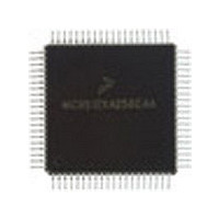
MC9S12C128VFU Freescale Semiconductor, MC9S12C128VFU Datasheet - Page 146

MC9S12C128VFU
Manufacturer Part Number
MC9S12C128VFU
Description
Manufacturer
Freescale Semiconductor
Datasheet
1.MC9S12C128VFU.pdf
(690 pages)
Specifications of MC9S12C128VFU
Cpu Family
HCS12
Device Core Size
16b
Frequency (max)
25MHz
Interface Type
CAN/SCI/SPI
Program Memory Type
Flash
Program Memory Size
128KB
Total Internal Ram Size
4KB
# I/os (max)
60
Number Of Timers - General Purpose
8
Operating Supply Voltage (typ)
2.5/5V
Operating Supply Voltage (max)
2.75/5.5V
Operating Supply Voltage (min)
2.35/2.97V
On-chip Adc
8-chx10-bit
Instruction Set Architecture
CISC
Operating Temp Range
-40C to 105C
Operating Temperature Classification
Industrial
Mounting
Surface Mount
Pin Count
80
Package Type
PQFP
Lead Free Status / Rohs Status
Not Compliant
Available stocks
Company
Part Number
Manufacturer
Quantity
Price
Company:
Part Number:
MC9S12C128VFUE
Manufacturer:
Freescale
Quantity:
38 000
Company:
Part Number:
MC9S12C128VFUE
Manufacturer:
Freescale Semiconductor
Quantity:
10 000
- Current page: 146 of 690
- Download datasheet (4Mb)
Chapter 4 Multiplexed External Bus Interface (MEBIV3)
This register is not in the on-chip memory map in expanded and special peripheral modes. Therefore, these
accesses will be echoed externally.
4.3.2.11
Read: Anytime (provided this register is in the map)
Write: Anytime (provided this register is in the map)
This register is used to select reduced drive for the pins associated with the core ports. This gives reduced
power consumption and reduced RFI with a slight increase in transition time (depending on loading). This
feature would be used on ports which have a light loading. The reduced drive function is independent of
which function is being used on a particular port.
This register is not in the on-chip memory map in expanded and special peripheral modes. Therefore, these
accesses will be echoed externally.
146
Module Base + 0x000D
Starting address location affected by INITRG register setting.
PUPKE
PUPEE
PUPBE
PUPAE
Field
7
4
1
0
Reset
W
R
Pull resistors Port K Enable
0 Port K pull resistors are disabled.
1 Enable pull resistors for port K input pins.
Pull resistors Port E Enable
0 Port E pull resistors on bits 7, 4:0 are disabled.
1 Enable pull resistors for port E input pins bits 7, 4:0.
Note: Pins 5 and 6 of port E have pull resistors which are only enabled during reset. This bit has no effect on
Pull resistors Port B Enable
0 Port B pull resistors are disabled.
1 Enable pull resistors for all port B input pins.
Pull resistors Port A Enable
0 Port A pull resistors are disabled.
1 Enable pull resistors for all port A input pins.
Reduced Drive Register (RDRIV)
RDRK
These bits have no effect when the associated pin(s) are outputs. (The pull
resistors are inactive.)
0
7
these pins.
= Unimplemented or Reserved
0
0
6
Figure 4-15. Reduced Drive Register (RDRIV)
Table 4-9. PUCR Field Descriptions
MC9S12C-Family / MC9S12GC-Family
0
0
5
Rev 01.24
NOTE
RDPE
0
4
Description
3
0
0
2
0
0
Freescale Semiconductor
RDPB
0
1
RDPA
0
0
Related parts for MC9S12C128VFU
Image
Part Number
Description
Manufacturer
Datasheet
Request
R
Part Number:
Description:
Manufacturer:
Freescale Semiconductor, Inc
Datasheet:
Part Number:
Description:
Manufacturer:
Freescale Semiconductor, Inc
Datasheet:
Part Number:
Description:
Manufacturer:
Freescale Semiconductor, Inc
Datasheet:
Part Number:
Description:
Manufacturer:
Freescale Semiconductor, Inc
Datasheet:
Part Number:
Description:
Manufacturer:
Freescale Semiconductor, Inc
Datasheet:
Part Number:
Description:
Manufacturer:
Freescale Semiconductor, Inc
Datasheet:
Part Number:
Description:
Manufacturer:
Freescale Semiconductor, Inc
Datasheet:
Part Number:
Description:
Manufacturer:
Freescale Semiconductor, Inc
Datasheet:
Part Number:
Description:
Manufacturer:
Freescale Semiconductor, Inc
Datasheet:
Part Number:
Description:
Manufacturer:
Freescale Semiconductor, Inc
Datasheet:
Part Number:
Description:
Manufacturer:
Freescale Semiconductor, Inc
Datasheet:
Part Number:
Description:
Manufacturer:
Freescale Semiconductor, Inc
Datasheet:
Part Number:
Description:
Manufacturer:
Freescale Semiconductor, Inc
Datasheet:
Part Number:
Description:
Manufacturer:
Freescale Semiconductor, Inc
Datasheet:
Part Number:
Description:
Manufacturer:
Freescale Semiconductor, Inc
Datasheet:


