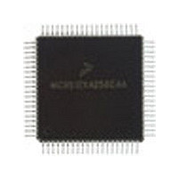
MC9S12C128VFU Freescale Semiconductor, MC9S12C128VFU Datasheet - Page 378

MC9S12C128VFU
Manufacturer Part Number
MC9S12C128VFU
Description
Manufacturer
Freescale Semiconductor
Datasheet
1.MC9S12C128VFU.pdf
(690 pages)
Specifications of MC9S12C128VFU
Cpu Family
HCS12
Device Core Size
16b
Frequency (max)
25MHz
Interface Type
CAN/SCI/SPI
Program Memory Type
Flash
Program Memory Size
128KB
Total Internal Ram Size
4KB
# I/os (max)
60
Number Of Timers - General Purpose
8
Operating Supply Voltage (typ)
2.5/5V
Operating Supply Voltage (max)
2.75/5.5V
Operating Supply Voltage (min)
2.35/2.97V
On-chip Adc
8-chx10-bit
Instruction Set Architecture
CISC
Operating Temp Range
-40C to 105C
Operating Temperature Classification
Industrial
Mounting
Surface Mount
Pin Count
80
Package Type
PQFP
Lead Free Status / Rohs Status
Not Compliant
Available stocks
Company
Part Number
Manufacturer
Quantity
Price
Company:
Part Number:
MC9S12C128VFUE
Manufacturer:
Freescale
Quantity:
38 000
Company:
Part Number:
MC9S12C128VFUE
Manufacturer:
Freescale Semiconductor
Quantity:
10 000
- Current page: 378 of 690
- Download datasheet (4Mb)
Chapter 12 Pulse-Width Modulator (PWM8B6CV1) Block Description
Shown below is the output waveform generated.
12.4.2.6
For center aligned output mode selection, set the CAEx bit (CAEx = 1) in the PWMCAE register and the
corresponding PWM output will be center aligned.
The 8-bit counter operates as an up/down counter in this mode and is set to up whenever the counter is
equal to 0x0000. The counter compares to two registers, a duty register and a period register as shown in
the block diagram in
changes state causing the PWM waveform to also change state. A match between the PWM counter and
the period register changes the counter direction from an up-count to a down-count. When the PWM
counter decrements and matches the duty register again, the output flip-flop changes state causing the
PWM output to also change state. When the PWM counter decrements and reaches 0, the counter direction
changes from a down-count back to an up-count and a load from the double buffer period and duty
registers to the associated registers is performed as described in
Duty.”
effective period is PWMPERx*2.
378
The counter counts from 0 up to the value in the period register and then back down to 0. Thus the
PPOLx = 0
PPOLx = 1
Center Aligned Outputs
Changing the PWM output mode from left aligned output to center aligned
output (or vice versa) while channels are operating can cause irregularities
in the PWM output. It is recommended to program the output mode before
enabling the PWM channel.
Figure
E = 100 ns
Figure 12-37. PWM Left Aligned Output Example Waveform
Figure 12-38. PWM Center Aligned Output Waveform
12-35. When the PWM counter matches the duty register the output flip-flop
PWMDTYx
MC9S12C-Family / MC9S12GC-Family
PWMPERx
PERIOD = 400 ns
DUTY CYCLE = 75%
Rev 01.24
NOTE
Period = PWMPERx*2
Section 12.4.2.3, “PWM Period and
PWMPERx
PWMDTYx
Freescale Semiconductor
Related parts for MC9S12C128VFU
Image
Part Number
Description
Manufacturer
Datasheet
Request
R
Part Number:
Description:
Manufacturer:
Freescale Semiconductor, Inc
Datasheet:
Part Number:
Description:
Manufacturer:
Freescale Semiconductor, Inc
Datasheet:
Part Number:
Description:
Manufacturer:
Freescale Semiconductor, Inc
Datasheet:
Part Number:
Description:
Manufacturer:
Freescale Semiconductor, Inc
Datasheet:
Part Number:
Description:
Manufacturer:
Freescale Semiconductor, Inc
Datasheet:
Part Number:
Description:
Manufacturer:
Freescale Semiconductor, Inc
Datasheet:
Part Number:
Description:
Manufacturer:
Freescale Semiconductor, Inc
Datasheet:
Part Number:
Description:
Manufacturer:
Freescale Semiconductor, Inc
Datasheet:
Part Number:
Description:
Manufacturer:
Freescale Semiconductor, Inc
Datasheet:
Part Number:
Description:
Manufacturer:
Freescale Semiconductor, Inc
Datasheet:
Part Number:
Description:
Manufacturer:
Freescale Semiconductor, Inc
Datasheet:
Part Number:
Description:
Manufacturer:
Freescale Semiconductor, Inc
Datasheet:
Part Number:
Description:
Manufacturer:
Freescale Semiconductor, Inc
Datasheet:
Part Number:
Description:
Manufacturer:
Freescale Semiconductor, Inc
Datasheet:
Part Number:
Description:
Manufacturer:
Freescale Semiconductor, Inc
Datasheet:


