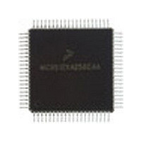
MC9S12C128VFU Freescale Semiconductor, MC9S12C128VFU Datasheet - Page 207

MC9S12C128VFU
Manufacturer Part Number
MC9S12C128VFU
Description
Manufacturer
Freescale Semiconductor
Datasheet
1.MC9S12C128VFU.pdf
(690 pages)
Specifications of MC9S12C128VFU
Cpu Family
HCS12
Device Core Size
16b
Frequency (max)
25MHz
Interface Type
CAN/SCI/SPI
Program Memory Type
Flash
Program Memory Size
128KB
Total Internal Ram Size
4KB
# I/os (max)
60
Number Of Timers - General Purpose
8
Operating Supply Voltage (typ)
2.5/5V
Operating Supply Voltage (max)
2.75/5.5V
Operating Supply Voltage (min)
2.35/2.97V
On-chip Adc
8-chx10-bit
Instruction Set Architecture
CISC
Operating Temp Range
-40C to 105C
Operating Temperature Classification
Industrial
Mounting
Surface Mount
Pin Count
80
Package Type
PQFP
Lead Free Status / Rohs Status
Not Compliant
Available stocks
Company
Part Number
Manufacturer
Quantity
Price
Company:
Part Number:
MC9S12C128VFUE
Manufacturer:
Freescale
Quantity:
38 000
Company:
Part Number:
MC9S12C128VFUE
Manufacturer:
Freescale Semiconductor
Quantity:
10 000
- Current page: 207 of 690
- Download datasheet (4Mb)
Freescale Semiconductor
BKAMB[H:L]
BKBMB[H:L]
RWAEN
Field
RWA
7:6
5:4
3
2
Breakpoint Mask High Byte for First Address — In dual or full mode, these bits may be used to mask (disable)
the comparison of the high and/or low bytes of the first address breakpoint. The functionality is as given in
Table
The x:0 case is for a full address compare. When a program page is selected, the full address compare will be
based on bits for a 20-bit compare. The registers used for the compare are {DBGCAX[5:0], DBGCAH[5:0],
DBGCAL[7:0]}, where DBGAX[5:0] corresponds to PPAGE[5:0] or extended address bits [19:14] and CPU
address [13:0]. When a program page is not selected, the full address compare will be based on bits for a 16-bit
compare. The registers used for the compare are {DBGCAH[7:0], DBGCAL[7:0]} which corresponds to CPU
address [15:0].
Note: This extended address compare scheme causes an aliasing problem in BKP mode in which several
The 1:0 case is not sensible because it would ignore the high order address and compare the low order and
expansion addresses. Logic forces this case to compare all address lines (effectively ignoring the BKAMBH
control bit).
The 1:1 case is useful for triggering a breakpoint on any access to a particular expansion page. This only makes
sense if a program page is being accessed so that the breakpoint trigger will occur only if DBGCAX compares.
Breakpoint Mask High Byte and Low Byte of Data (Second Address) — In dual mode, these bits may be
used to mask (disable) the comparison of the high and/or low bytes of the second address breakpoint. The
functionality is as given in
The x:0 case is for a full address compare. When a program page is selected, the full address compare will be
based on bits for a 20-bit compare. The registers used for the compare are {DBGCBX[5:0], DBGCBH[5:0],
DBGCBL[7:0]} where DBGCBX[5:0] corresponds to PPAGE[5:0] or extended address bits [19:14] and CPU
address [13:0]. When a program page is not selected, the full address compare will be based on bits for a 16-bit
compare. The registers used for the compare are {DBGCBH[7:0], DBGCBL[7:0]} which corresponds to CPU
address [15:0].
Note: This extended address compare scheme causes an aliasing problem in BKP mode in which several
The 1:0 case is not sensible because it would ignore the high order address and compare the low order and
expansion addresses. Logic forces this case to compare all address lines (effectively ignoring the BKBMBH
control bit).
The 1:1 case is useful for triggering a breakpoint on any access to a particular expansion page. This only makes
sense if a program page is being accessed so that the breakpoint trigger will occur only if DBGCBX compares.
In full mode, these bits may be used to mask (disable) the comparison of the high and/or low bytes of the data
breakpoint. The functionality is as given in
Read/Write Comparator A Enable Bit — The RWAEN bit controls whether read or write comparison is enabled
for comparator A. See
for tagged operations.
0 Read/Write is not used in comparison
1 Read/Write is used in comparison
Read/Write Comparator A Value Bit — The RWA bit controls whether read or write is used in compare for
comparator A. The RWA bit is not used if RWAEN = 0.
0 Write cycle will be matched
1 Read cycle will be matched
7-16.
physical addresses may match with a single logical address. This problem may be avoided by using DBG
mode to generate breakpoints.
physical addresses may match with a single logical address. This problem may be avoided by using DBG
mode to generate breakpoints.
Section 7.4.2.1.1, “Read or Write
Table 7-15. DBGC3 Field Descriptions
Table
MC9S12C-Family / MC9S12GC-Family
7-17.
Table
Rev 01.24
7-18.
Description
Comparison,” for more information. This bit is not useful
Chapter 7 Debug Module (DBGV1) Block Description
207
Related parts for MC9S12C128VFU
Image
Part Number
Description
Manufacturer
Datasheet
Request
R
Part Number:
Description:
Manufacturer:
Freescale Semiconductor, Inc
Datasheet:
Part Number:
Description:
Manufacturer:
Freescale Semiconductor, Inc
Datasheet:
Part Number:
Description:
Manufacturer:
Freescale Semiconductor, Inc
Datasheet:
Part Number:
Description:
Manufacturer:
Freescale Semiconductor, Inc
Datasheet:
Part Number:
Description:
Manufacturer:
Freescale Semiconductor, Inc
Datasheet:
Part Number:
Description:
Manufacturer:
Freescale Semiconductor, Inc
Datasheet:
Part Number:
Description:
Manufacturer:
Freescale Semiconductor, Inc
Datasheet:
Part Number:
Description:
Manufacturer:
Freescale Semiconductor, Inc
Datasheet:
Part Number:
Description:
Manufacturer:
Freescale Semiconductor, Inc
Datasheet:
Part Number:
Description:
Manufacturer:
Freescale Semiconductor, Inc
Datasheet:
Part Number:
Description:
Manufacturer:
Freescale Semiconductor, Inc
Datasheet:
Part Number:
Description:
Manufacturer:
Freescale Semiconductor, Inc
Datasheet:
Part Number:
Description:
Manufacturer:
Freescale Semiconductor, Inc
Datasheet:
Part Number:
Description:
Manufacturer:
Freescale Semiconductor, Inc
Datasheet:
Part Number:
Description:
Manufacturer:
Freescale Semiconductor, Inc
Datasheet:


