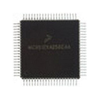
MC9S12C128VFU Freescale Semiconductor, MC9S12C128VFU Datasheet - Page 56

MC9S12C128VFU
Manufacturer Part Number
MC9S12C128VFU
Description
Manufacturer
Freescale Semiconductor
Datasheet
1.MC9S12C128VFU.pdf
(690 pages)
Specifications of MC9S12C128VFU
Cpu Family
HCS12
Device Core Size
16b
Frequency (max)
25MHz
Interface Type
CAN/SCI/SPI
Program Memory Type
Flash
Program Memory Size
128KB
Total Internal Ram Size
4KB
# I/os (max)
60
Number Of Timers - General Purpose
8
Operating Supply Voltage (typ)
2.5/5V
Operating Supply Voltage (max)
2.75/5.5V
Operating Supply Voltage (min)
2.35/2.97V
On-chip Adc
8-chx10-bit
Instruction Set Architecture
CISC
Operating Temp Range
-40C to 105C
Operating Temperature Classification
Industrial
Mounting
Surface Mount
Pin Count
80
Package Type
PQFP
Lead Free Status / Rohs Status
Not Compliant
Available stocks
Company
Part Number
Manufacturer
Quantity
Price
Company:
Part Number:
MC9S12C128VFUE
Manufacturer:
Freescale
Quantity:
38 000
Company:
Part Number:
MC9S12C128VFUE
Manufacturer:
Freescale Semiconductor
Quantity:
10 000
- Current page: 56 of 690
- Download datasheet (4Mb)
Chapter 1 MC9S12C and MC9S12GC Device Overview (MC9S12C128)
1.3.5.4
V
to digital converter.
1.3.5.5
V
1.3.5.6
Provides operating voltage and ground for the oscillator and the phased-locked loop. This allows the
supply voltage to the oscillator and PLL to be bypassed independently. This 2.5V voltage is generated by
the internal voltage regulator.
56
Mnemonic
V
DDA
RH
V
DD1, VDD2
SS1, VSS2
V
V
V
V
V
V
V
V
V
DDPLL
SSPLL
V
and V
DDR
SSR
DDX
SSX
DDA
SSA
RH
RL
, V
SSA
RL
are the power supply and ground input pins for the voltage regulator reference and the analog
V
V
V
Voltage (V)
are the reference voltage input pins for the analog to digital converter.
Nominal
All V
signal transitions place high, short-duration current demands on the power
supply, use bypass capacitors with high-frequency characteristics and place
them as close to the MCU as possible. Bypass requirements depend on
MCU pin load.
DDA
RH
DDPLL
2.5
5.0
5.0
5.0
5.0
2.5
0
0
0
0
0
0
, V
, V
SS
RL
, V
SSA
pins must be connected together in the application. Because fast
Internal power and ground generated by internal regulator. These also allow an external source
to supply the core V
In the 48 and 52 LQFP packages V
External power and ground, supply to internal voltage regulator.
External power and ground, supply to pin drivers.
Operating voltage and ground for the analog-to-digital converters and the reference for the
internal voltage regulator, allows the supply voltage to the A/D to be bypassed independently.
Reference voltage low for the ATD converter.
In the 48 and 52 LQFP packages V
Provides operating voltage and ground for the phased-locked loop. This allows the supply voltage
to the PLL to be bypassed independently. Internal power and ground generated by internal
regulator.
— ATD Reference Voltage Input Pins
SSPLL
Table 1-6. Power and Ground Connection Summary
— Power Supply Pins for ATD and VREG
— Power Supply Pins for PLL
MC9S12C-Family / MC9S12GC-Family
DD
/V
SS
voltages and bypass the internal voltage regulator.
Rev 01.24
NOTE
DD2
RL
is bonded to V
and V
Description
SS2
are not available.
SSA
.
Freescale Semiconductor
Related parts for MC9S12C128VFU
Image
Part Number
Description
Manufacturer
Datasheet
Request
R
Part Number:
Description:
Manufacturer:
Freescale Semiconductor, Inc
Datasheet:
Part Number:
Description:
Manufacturer:
Freescale Semiconductor, Inc
Datasheet:
Part Number:
Description:
Manufacturer:
Freescale Semiconductor, Inc
Datasheet:
Part Number:
Description:
Manufacturer:
Freescale Semiconductor, Inc
Datasheet:
Part Number:
Description:
Manufacturer:
Freescale Semiconductor, Inc
Datasheet:
Part Number:
Description:
Manufacturer:
Freescale Semiconductor, Inc
Datasheet:
Part Number:
Description:
Manufacturer:
Freescale Semiconductor, Inc
Datasheet:
Part Number:
Description:
Manufacturer:
Freescale Semiconductor, Inc
Datasheet:
Part Number:
Description:
Manufacturer:
Freescale Semiconductor, Inc
Datasheet:
Part Number:
Description:
Manufacturer:
Freescale Semiconductor, Inc
Datasheet:
Part Number:
Description:
Manufacturer:
Freescale Semiconductor, Inc
Datasheet:
Part Number:
Description:
Manufacturer:
Freescale Semiconductor, Inc
Datasheet:
Part Number:
Description:
Manufacturer:
Freescale Semiconductor, Inc
Datasheet:
Part Number:
Description:
Manufacturer:
Freescale Semiconductor, Inc
Datasheet:
Part Number:
Description:
Manufacturer:
Freescale Semiconductor, Inc
Datasheet:


