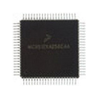
MC9S12C128VFU Freescale Semiconductor, MC9S12C128VFU Datasheet - Page 54

MC9S12C128VFU
Manufacturer Part Number
MC9S12C128VFU
Description
Manufacturer
Freescale Semiconductor
Datasheet
1.MC9S12C128VFU.pdf
(690 pages)
Specifications of MC9S12C128VFU
Cpu Family
HCS12
Device Core Size
16b
Frequency (max)
25MHz
Interface Type
CAN/SCI/SPI
Program Memory Type
Flash
Program Memory Size
128KB
Total Internal Ram Size
4KB
# I/os (max)
60
Number Of Timers - General Purpose
8
Operating Supply Voltage (typ)
2.5/5V
Operating Supply Voltage (max)
2.75/5.5V
Operating Supply Voltage (min)
2.35/2.97V
On-chip Adc
8-chx10-bit
Instruction Set Architecture
CISC
Operating Temp Range
-40C to 105C
Operating Temperature Classification
Industrial
Mounting
Surface Mount
Pin Count
80
Package Type
PQFP
Lead Free Status / Rohs Status
Not Compliant
Available stocks
Company
Part Number
Manufacturer
Quantity
Price
Company:
Part Number:
MC9S12C128VFUE
Manufacturer:
Freescale
Quantity:
38 000
Company:
Part Number:
MC9S12C128VFUE
Manufacturer:
Freescale Semiconductor
Quantity:
10 000
- Current page: 54 of 690
- Download datasheet (4Mb)
Chapter 1 MC9S12C and MC9S12GC Device Overview (MC9S12C128)
the Flash EEPROM memory in the memory map (ROMCTL). At the rising edge of RESET, the state of
this pin is latched to the ROMON bit.
1.3.4.19
PP[5:0] are general purpose input or output pins, shared with the keypad interrupt function. When
configured as inputs, they can generate interrupts causing the MCU to exit stop or wait mode.
PP[5:0] are also shared with the PWM output signals, PW[5:0]. Pins PP[2:0] are only available in the 80-
pin package version. Pins PP[4:3] are not available in the 48-pin package version.
1.3.4.20
PJ[7:6] are general purpose input or output pins, shared with the keypad interrupt function. When
configured as inputs, they can generate interrupts causing the MCU to exit stop or wait mode. These pins
are not available in the 48-pin package version nor in the 52-pin package version.
1.3.4.21
PM5 is a general purpose input or output pin and also the serial clock pin SCK for the serial peripheral
interface (SPI).
1.3.4.22
PM4 is a general purpose input or output pin and also the master output (during master mode) or slave
input (during slave mode) pin for the serial peripheral interface (SPI).
1.3.4.23
PM3 is a general purpose input or output pin and also the slave select pin SS for the serial peripheral
interface (SPI).
1.3.4.24
PM2 is a general purpose input or output pin and also the master input (during master mode) or slave
output (during slave mode) pin for the serial peripheral interface (SPI).
1.3.4.25
PM1 is a general purpose input or output pin and the transmit pin, TXCAN, of the CAN module if
available.
1.3.4.26
PM0 is a general purpose input or output pin and the receive pin, RXCAN, of the CAN module if available.
54
•
•
PP6 = 1 in emulation modes equates to ROMON = 0 (ROM space externally mapped)
PP6 = 0 in expanded modes equates to ROMON = 0 (ROM space externally mapped)
PP[5:0] / KWP[5:0] / PW[5:0] — Port P I/O Pins [5:0]
PJ[7:6] / KWJ[7:6] — Port J I/O Pins [7:6]
PM5 / SCK — Port M I/O Pin 5
PM4 / MOSI — Port M I/O Pin 4
PM3 / SS — Port M I/O Pin 3
PM2 / MISO — Port M I/O Pin 2
PM1 / TXCAN — Port M I/O Pin 1
PM0 / RXCAN — Port M I/O Pin 0
MC9S12C-Family / MC9S12GC-Family
Rev 01.24
Freescale Semiconductor
Related parts for MC9S12C128VFU
Image
Part Number
Description
Manufacturer
Datasheet
Request
R
Part Number:
Description:
Manufacturer:
Freescale Semiconductor, Inc
Datasheet:
Part Number:
Description:
Manufacturer:
Freescale Semiconductor, Inc
Datasheet:
Part Number:
Description:
Manufacturer:
Freescale Semiconductor, Inc
Datasheet:
Part Number:
Description:
Manufacturer:
Freescale Semiconductor, Inc
Datasheet:
Part Number:
Description:
Manufacturer:
Freescale Semiconductor, Inc
Datasheet:
Part Number:
Description:
Manufacturer:
Freescale Semiconductor, Inc
Datasheet:
Part Number:
Description:
Manufacturer:
Freescale Semiconductor, Inc
Datasheet:
Part Number:
Description:
Manufacturer:
Freescale Semiconductor, Inc
Datasheet:
Part Number:
Description:
Manufacturer:
Freescale Semiconductor, Inc
Datasheet:
Part Number:
Description:
Manufacturer:
Freescale Semiconductor, Inc
Datasheet:
Part Number:
Description:
Manufacturer:
Freescale Semiconductor, Inc
Datasheet:
Part Number:
Description:
Manufacturer:
Freescale Semiconductor, Inc
Datasheet:
Part Number:
Description:
Manufacturer:
Freescale Semiconductor, Inc
Datasheet:
Part Number:
Description:
Manufacturer:
Freescale Semiconductor, Inc
Datasheet:
Part Number:
Description:
Manufacturer:
Freescale Semiconductor, Inc
Datasheet:


