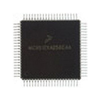
MC9S12C128VFU Freescale Semiconductor, MC9S12C128VFU Datasheet - Page 400

MC9S12C128VFU
Manufacturer Part Number
MC9S12C128VFU
Description
Manufacturer
Freescale Semiconductor
Datasheet
1.MC9S12C128VFU.pdf
(690 pages)
Specifications of MC9S12C128VFU
Cpu Family
HCS12
Device Core Size
16b
Frequency (max)
25MHz
Interface Type
CAN/SCI/SPI
Program Memory Type
Flash
Program Memory Size
128KB
Total Internal Ram Size
4KB
# I/os (max)
60
Number Of Timers - General Purpose
8
Operating Supply Voltage (typ)
2.5/5V
Operating Supply Voltage (max)
2.75/5.5V
Operating Supply Voltage (min)
2.35/2.97V
On-chip Adc
8-chx10-bit
Instruction Set Architecture
CISC
Operating Temp Range
-40C to 105C
Operating Temperature Classification
Industrial
Mounting
Surface Mount
Pin Count
80
Package Type
PQFP
Lead Free Status / Rohs Status
Not Compliant
Available stocks
Company
Part Number
Manufacturer
Quantity
Price
Company:
Part Number:
MC9S12C128VFUE
Manufacturer:
Freescale
Quantity:
38 000
Company:
Part Number:
MC9S12C128VFUE
Manufacturer:
Freescale Semiconductor
Quantity:
10 000
- Current page: 400 of 690
- Download datasheet (4Mb)
Chapter 13 Serial Communications Interface (S12SCIV2) Block Description
13.4.4
13.4.4.1
The SCI receiver can accommodate either 8-bit or 9-bit data characters. The state of the M bit in SCI
control register 1 (SCICR1) determines the length of data characters. When receiving 9-bit data, bit R8 in
SCI data register high (SCIDRH) is the ninth bit (bit 8).
400
FROM TXD
RXD
LOOPS
RSRC
Receiver
Receiver Character Length
When queueing an idle character, return the TE bit to logic 1 before the stop
bit of the current frame shifts out through the Tx output signal. Setting TE
after the stop bit appears on Tx output signal causes data previously written
to the SCI data register to be lost. Toggle the TE bit for a queued idle
character while the TDRE flag is set and immediately before writing the
next byte to the SCI data register.
If the TE bit is clear and the transmission is complete, the SCI is not the
master of the TXD pin
RDRF/OR INTERRUPT REQUEST
CONTROL
IDLE INTERRUPT REQUEST
LOOP
CLOCK
SBR12–SBR0
BUS
BAUD DIVIDER
Figure 13-12. SCI Receiver Block Diagram
WAKE
RAF
RE
ILT
PE
PT
M
MC9S12C-Family / MC9S12GC-Family
RECOVERY
DATA
CHECKING
WAKEUP
PARITY
LOGIC
Rev 01.24
NOTE
NOTE
INTERNAL BUS
IDLE
ILIE
RIE
H
8
11-BIT RECEIVE SHIFT REGISTER
7
RDRF
SCI DATA REGISTER
OR
6
5
4
R8
FE
NF
PE
3
Freescale Semiconductor
2
1
0
L
RWU
Related parts for MC9S12C128VFU
Image
Part Number
Description
Manufacturer
Datasheet
Request
R
Part Number:
Description:
Manufacturer:
Freescale Semiconductor, Inc
Datasheet:
Part Number:
Description:
Manufacturer:
Freescale Semiconductor, Inc
Datasheet:
Part Number:
Description:
Manufacturer:
Freescale Semiconductor, Inc
Datasheet:
Part Number:
Description:
Manufacturer:
Freescale Semiconductor, Inc
Datasheet:
Part Number:
Description:
Manufacturer:
Freescale Semiconductor, Inc
Datasheet:
Part Number:
Description:
Manufacturer:
Freescale Semiconductor, Inc
Datasheet:
Part Number:
Description:
Manufacturer:
Freescale Semiconductor, Inc
Datasheet:
Part Number:
Description:
Manufacturer:
Freescale Semiconductor, Inc
Datasheet:
Part Number:
Description:
Manufacturer:
Freescale Semiconductor, Inc
Datasheet:
Part Number:
Description:
Manufacturer:
Freescale Semiconductor, Inc
Datasheet:
Part Number:
Description:
Manufacturer:
Freescale Semiconductor, Inc
Datasheet:
Part Number:
Description:
Manufacturer:
Freescale Semiconductor, Inc
Datasheet:
Part Number:
Description:
Manufacturer:
Freescale Semiconductor, Inc
Datasheet:
Part Number:
Description:
Manufacturer:
Freescale Semiconductor, Inc
Datasheet:
Part Number:
Description:
Manufacturer:
Freescale Semiconductor, Inc
Datasheet:


