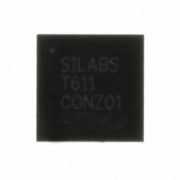
C8051T611-GM Silicon Laboratories Inc, C8051T611-GM Datasheet - Page 102

C8051T611-GM
Manufacturer Part Number
C8051T611-GM
Description
IC 8051 MCU 16K BYTE-PROG 28-QFN
Manufacturer
Silicon Laboratories Inc
Series
C8051T61xr
Specifications of C8051T611-GM
Core Processor
8051
Core Size
8-Bit
Speed
25MHz
Connectivity
SMBus (2-Wire/I²C), SPI, UART/USART
Peripherals
POR, PWM, Temp Sensor, WDT
Number Of I /o
25
Program Memory Size
16KB (16K x 8)
Program Memory Type
OTP
Ram Size
1.25K x 8
Voltage - Supply (vcc/vdd)
1.8 V ~ 3.6 V
Data Converters
A/D 17x10b
Oscillator Type
Internal
Operating Temperature
-40°C ~ 85°C
Package / Case
28-QFN
Processor Series
C8051T6x
Core
8051
Data Bus Width
8 bit
Data Ram Size
1.25 KB
Interface Type
I2C, SPI, UART
Maximum Clock Frequency
25 MHz
Number Of Programmable I/os
29
Number Of Timers
4
Maximum Operating Temperature
+ 85 C
Mounting Style
SMD/SMT
3rd Party Development Tools
PK51, CA51, A51, ULINK2
Development Tools By Supplier
C8051FT610DK
Minimum Operating Temperature
- 40 C
On-chip Adc
10 bit, 21 Channel
Lead Free Status / RoHS Status
Lead free / RoHS Compliant
Eeprom Size
-
Lead Free Status / Rohs Status
Details
Other names
336-1436-5
Available stocks
Company
Part Number
Manufacturer
Quantity
Price
Company:
Part Number:
C8051T611-GM
Manufacturer:
Silicon Labs
Quantity:
135
Company:
Part Number:
C8051T611-GMR
Manufacturer:
SILICON
Quantity:
3 500
Part Number:
C8051T611-GMR
Manufacturer:
SILICON LABS/芯科
Quantity:
20 000
C8051T610/1/2/3/4/5/6/7
19.2. Power-Fail Reset/V
When a power-down transition or power irregularity causes V
monitor will drive the RST pin low and hold the CIP-51 in a reset state (see Figure 19.2). When V
to a level above V
memory contents are not altered by the power-fail reset, it is impossible to determine if V
the level required for data retention. If the PORSF flag reads 1, the data may no longer be valid. The V
monitor is enabled after power-on resets. Its defined state (enabled/disabled) is not altered by any other
reset source. For example, if the V
V
Important Note: If the V
is selected as a reset source. Selecting the V
lized may cause a system reset. In some applications, this reset may be undesirable. If this is not desirable
in the application, a delay should be introduced between enabling the monitor and selecting it as a reset
source. The procedure for enabling the V
state is shown below:
1. Enable the V
2. If necessary, wait for the V
3. Select the V
See Figure 19.2 for V
monitor reset. See Table 7.4 for complete electrical characteristics of the V
102
DD
monitor will still be disabled after the reset.
DD
DD
RST
monitor as a reset source (PORSF bit in RSTSRC = 1).
monitor (VDMEN bit in VDM0CN = 1).
, the CIP-51 will be released from the reset state. Note that even though internal data
DD
DD
monitor timing; note that the power-on-reset delay is not incurred after a V
monitor is being turned on from a disabled state, it should be enabled before it
DD
DD
monitor to stabilize (see Table 7.4 for the V
DD
Monitor
monitor is disabled by code and a software reset is performed, the
DD
monitor and configuring it as a reset source from a disabled
DD
monitor as a reset source before it is enabled and stabi-
Rev 1.0
DD
to drop below V
DD
DD
monitor.
Monitor turn-on time).
RST
, the power supply
DD
dropped below
DD
returns
DD
DD


