C8051T611-GM Silicon Laboratories Inc, C8051T611-GM Datasheet - Page 115
C8051T611-GM
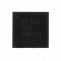
Manufacturer Part Number
C8051T611-GM
Description
IC 8051 MCU 16K BYTE-PROG 28-QFN
Manufacturer
Silicon Laboratories Inc
Series
C8051T61xr
Specifications of C8051T611-GM
Core Processor
8051
Core Size
8-Bit
Speed
25MHz
Connectivity
SMBus (2-Wire/I²C), SPI, UART/USART
Peripherals
POR, PWM, Temp Sensor, WDT
Number Of I /o
25
Program Memory Size
16KB (16K x 8)
Program Memory Type
OTP
Ram Size
1.25K x 8
Voltage - Supply (vcc/vdd)
1.8 V ~ 3.6 V
Data Converters
A/D 17x10b
Oscillator Type
Internal
Operating Temperature
-40°C ~ 85°C
Package / Case
28-QFN
Processor Series
C8051T6x
Core
8051
Data Bus Width
8 bit
Data Ram Size
1.25 KB
Interface Type
I2C, SPI, UART
Maximum Clock Frequency
25 MHz
Number Of Programmable I/os
29
Number Of Timers
4
Maximum Operating Temperature
+ 85 C
Mounting Style
SMD/SMT
3rd Party Development Tools
PK51, CA51, A51, ULINK2
Development Tools By Supplier
C8051FT610DK
Minimum Operating Temperature
- 40 C
On-chip Adc
10 bit, 21 Channel
Lead Free Status / RoHS Status
Lead free / RoHS Compliant
Eeprom Size
-
Lead Free Status / Rohs Status
Details
Other names
336-1436-5
Available stocks
Company
Part Number
Manufacturer
Quantity
Price
Company:

Part Number:
C8051T611-GM
Manufacturer:
Silicon Labs
Quantity:
135
Company:
Part Number:
C8051T611-GMR
Manufacturer:
SILICON
Quantity:
3 500
Part Number:
C8051T611-GMR
Manufacturer:
SILICON LABS/芯科
Quantity:
20 000


21.1.3. Interfacing Port I/O to 5V Logic
All Port I/O configured for digital, open-drain operation are capable of interfacing to digital logic operating at
a supply voltage higher than VDD and less than 5.25 V. An external pullup resistor to the higher supply
voltage on output pins is typically required for most systems.
Important Notes: The absolute maximum voltage of any Port I/O pin should be limited to VDD + 3.6V.
When interfacing to systems with supply voltages higher than 3.6V, care must be taken to limit the voltage
on I/O pins when the VDD supply to the device is not present. In a multi-voltage interface, the external pul-
lup resistor should be sized to allow a current of at least 150 µA to flow into the Port pin when the supply
voltage is between (VDD + 0.6 V) and (VDD + 1.0 V). Once the Port pin voltage increases beyond this
range, the current flowing into the Port pin is minimal.
WEAKPUD
(Weak Pull-Up Disable)
Px.x – Output
Logic Value
(Port Latch or
Crossbar)
PxMDOUT.x
(1 for push-pull)
(0 for open-drain)
XBARE
(Crossbar
Enable)
Px.x – Input Logic Value
(Reads 0 when pin is configured as an analog I/O)
To/From Analog
Peripheral
PxMDIN.x
(1 for digital)
(0 for analog)
Figure 21.2. Port I/O Cell Block Diagram
Rev 1.0
C8051T610/1/2/3/4/5/6/7
VDD
GND
VDD
(WEAK)
PORT
PAD
115
Related parts for C8051T611-GM
Image
Part Number
Description
Manufacturer
Datasheet
Request
R

Part Number:
Description:
SMD/C°/SINGLE-ENDED OUTPUT SILICON OSCILLATOR
Manufacturer:
Silicon Laboratories Inc
Part Number:
Description:
Manufacturer:
Silicon Laboratories Inc
Datasheet:
Part Number:
Description:
N/A N/A/SI4010 AES KEYFOB DEMO WITH LCD RX
Manufacturer:
Silicon Laboratories Inc
Datasheet:
Part Number:
Description:
N/A N/A/SI4010 SIMPLIFIED KEY FOB DEMO WITH LED RX
Manufacturer:
Silicon Laboratories Inc
Datasheet:
Part Number:
Description:
N/A/-40 TO 85 OC/EZLINK MODULE; F930/4432 HIGH BAND (REV E/B1)
Manufacturer:
Silicon Laboratories Inc
Part Number:
Description:
EZLink Module; F930/4432 Low Band (rev e/B1)
Manufacturer:
Silicon Laboratories Inc
Part Number:
Description:
I°/4460 10 DBM RADIO TEST CARD 434 MHZ
Manufacturer:
Silicon Laboratories Inc
Part Number:
Description:
I°/4461 14 DBM RADIO TEST CARD 868 MHZ
Manufacturer:
Silicon Laboratories Inc
Part Number:
Description:
I°/4463 20 DBM RFSWITCH RADIO TEST CARD 460 MHZ
Manufacturer:
Silicon Laboratories Inc
Part Number:
Description:
I°/4463 20 DBM RADIO TEST CARD 868 MHZ
Manufacturer:
Silicon Laboratories Inc
Part Number:
Description:
I°/4463 27 DBM RADIO TEST CARD 868 MHZ
Manufacturer:
Silicon Laboratories Inc
Part Number:
Description:
I°/4463 SKYWORKS 30 DBM RADIO TEST CARD 915 MHZ
Manufacturer:
Silicon Laboratories Inc
Part Number:
Description:
N/A N/A/-40 TO 85 OC/4463 RFMD 30 DBM RADIO TEST CARD 915 MHZ
Manufacturer:
Silicon Laboratories Inc
Part Number:
Description:
I°/4463 20 DBM RADIO TEST CARD 169 MHZ
Manufacturer:
Silicon Laboratories Inc