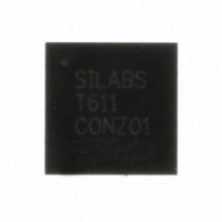
C8051T611-GM Silicon Laboratories Inc, C8051T611-GM Datasheet - Page 158

C8051T611-GM
Manufacturer Part Number
C8051T611-GM
Description
IC 8051 MCU 16K BYTE-PROG 28-QFN
Manufacturer
Silicon Laboratories Inc
Series
C8051T61xr
Specifications of C8051T611-GM
Core Processor
8051
Core Size
8-Bit
Speed
25MHz
Connectivity
SMBus (2-Wire/I²C), SPI, UART/USART
Peripherals
POR, PWM, Temp Sensor, WDT
Number Of I /o
25
Program Memory Size
16KB (16K x 8)
Program Memory Type
OTP
Ram Size
1.25K x 8
Voltage - Supply (vcc/vdd)
1.8 V ~ 3.6 V
Data Converters
A/D 17x10b
Oscillator Type
Internal
Operating Temperature
-40°C ~ 85°C
Package / Case
28-QFN
Processor Series
C8051T6x
Core
8051
Data Bus Width
8 bit
Data Ram Size
1.25 KB
Interface Type
I2C, SPI, UART
Maximum Clock Frequency
25 MHz
Number Of Programmable I/os
29
Number Of Timers
4
Maximum Operating Temperature
+ 85 C
Mounting Style
SMD/SMT
3rd Party Development Tools
PK51, CA51, A51, ULINK2
Development Tools By Supplier
C8051FT610DK
Minimum Operating Temperature
- 40 C
On-chip Adc
10 bit, 21 Channel
Lead Free Status / RoHS Status
Lead free / RoHS Compliant
Eeprom Size
-
Lead Free Status / Rohs Status
Details
Other names
336-1436-5
Available stocks
Company
Part Number
Manufacturer
Quantity
Price
Company:
Part Number:
C8051T611-GM
Manufacturer:
Silicon Labs
Quantity:
135
Company:
Part Number:
C8051T611-GMR
Manufacturer:
SILICON
Quantity:
3 500
Part Number:
C8051T611-GMR
Manufacturer:
SILICON LABS/芯科
Quantity:
20 000
C8051T610/1/2/3/4/5/6/7
24.1. Signal Descriptions
The four signals used by SPI0 (MOSI, MISO, SCK, NSS) are described below.
24.1.1. Master Out, Slave In (MOSI)
The master-out, slave-in (MOSI) signal is an output from a master device and an input to slave devices. It
is used to serially transfer data from the master to the slave. This signal is an output when SPI0 is operat-
ing as a master and an input when SPI0 is operating as a slave. Data is transferred most-significant bit
first. When configured as a master, MOSI is driven by the MSB of the shift register in both 3- and 4-wire
mode.
24.1.2. Master In, Slave Out (MISO)
The master-in, slave-out (MISO) signal is an output from a slave device and an input to the master device.
It is used to serially transfer data from the slave to the master. This signal is an input when SPI0 is operat-
ing as a master and an output when SPI0 is operating as a slave. Data is transferred most-significant bit
first. The MISO pin is placed in a high-impedance state when the SPI module is disabled and when the SPI
operates in 4-wire mode as a slave that is not selected. When acting as a slave in 3-wire mode, MISO is
always driven by the MSB of the shift register.
24.1.3. Serial Clock (SCK)
The serial clock (SCK) signal is an output from the master device and an input to slave devices. It is used
to synchronize the transfer of data between the master and slave on the MOSI and MISO lines. SPI0 gen-
erates this signal when operating as a master. The SCK signal is ignored by a SPI slave when the slave is
not selected (NSS = 1) in 4-wire slave mode.
24.1.4. Slave Select (NSS)
The function of the slave-select (NSS) signal is dependent on the setting of the NSSMD1 and NSSMD0
bits in the SPI0CN register. There are three possible modes that can be selected with these bits:
1. NSSMD[1:0] = 00: 3-Wire Master or 3-Wire Slave Mode: SPI0 operates in 3-wire mode, and NSS is
2. NSSMD[1:0] = 01: 4-Wire Slave or Multi-Master Mode: SPI0 operates in 4-wire mode, and NSS is
3. NSSMD[1:0] = 1x: 4-Wire Master Mode: SPI0 operates in 4-wire mode, and NSS is enabled as an
See Figure 24.2, Figure 24.3, and Figure 24.4 for typical connection diagrams of the various operational
modes. Note that the setting of NSSMD bits affects the pinout of the device. When in 3-wire master or
3-wire slave mode, the NSS pin will not be mapped by the crossbar. In all other modes, the NSS signal will
be mapped to a pin on the device. See Section “21. Port Input/Output” on page 113 for general purpose
port I/O and crossbar information.
158
disabled. When operating as a slave device, SPI0 is always selected in 3-wire mode. Since no select
signal is present, SPI0 must be the only slave on the bus in 3-wire mode. This is intended for point-to-
point communication between a master and one slave.
enabled as an input. When operating as a slave, NSS selects the SPI0 device. When operating as a
master, a 1-to-0 transition of the NSS signal disables the master function of SPI0 so that multiple
master devices can be used on the same SPI bus.
output. The setting of NSSMD0 determines what logic level the NSS pin will output. This configuration
should only be used when operating SPI0 as a master device.
Rev 1.0


