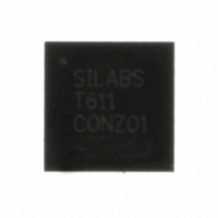
C8051T611-GM Silicon Laboratories Inc, C8051T611-GM Datasheet - Page 39

C8051T611-GM
Manufacturer Part Number
C8051T611-GM
Description
IC 8051 MCU 16K BYTE-PROG 28-QFN
Manufacturer
Silicon Laboratories Inc
Series
C8051T61xr
Specifications of C8051T611-GM
Core Processor
8051
Core Size
8-Bit
Speed
25MHz
Connectivity
SMBus (2-Wire/I²C), SPI, UART/USART
Peripherals
POR, PWM, Temp Sensor, WDT
Number Of I /o
25
Program Memory Size
16KB (16K x 8)
Program Memory Type
OTP
Ram Size
1.25K x 8
Voltage - Supply (vcc/vdd)
1.8 V ~ 3.6 V
Data Converters
A/D 17x10b
Oscillator Type
Internal
Operating Temperature
-40°C ~ 85°C
Package / Case
28-QFN
Processor Series
C8051T6x
Core
8051
Data Bus Width
8 bit
Data Ram Size
1.25 KB
Interface Type
I2C, SPI, UART
Maximum Clock Frequency
25 MHz
Number Of Programmable I/os
29
Number Of Timers
4
Maximum Operating Temperature
+ 85 C
Mounting Style
SMD/SMT
3rd Party Development Tools
PK51, CA51, A51, ULINK2
Development Tools By Supplier
C8051FT610DK
Minimum Operating Temperature
- 40 C
On-chip Adc
10 bit, 21 Channel
Lead Free Status / RoHS Status
Lead free / RoHS Compliant
Eeprom Size
-
Lead Free Status / Rohs Status
Details
Other names
336-1436-5
Available stocks
Company
Part Number
Manufacturer
Quantity
Price
Company:
Part Number:
C8051T611-GM
Manufacturer:
Silicon Labs
Quantity:
135
Company:
Part Number:
C8051T611-GMR
Manufacturer:
SILICON
Quantity:
3 500
Part Number:
C8051T611-GMR
Manufacturer:
SILICON LABS/芯科
Quantity:
20 000
8. 10-Bit ADC (ADC0, C8051T610/1/2/3/6 only)
ADC0 on the C8051T610/1/2/3/6 is a 500 ksps, 10-bit successive-approximation-register (SAR) ADC with
integrated track-and-hold, a gain stage programmable to 1x or 0.5x, and a programmable window detector.
The ADC is fully configurable under software control via Special Function Registers. The ADC may be con-
figured to measure various different signals using the analog multiplexer described in Section “8.5. ADC0
Analog Multiplexer (C8051T610/1/2/3/6 only)” on page 49. The voltage reference for the ADC is selected
as described in Section “10. Voltage Reference Options” on page 54. The ADC0 subsystem is enabled
only when the AD0EN bit in the ADC0 Control register (ADC0CN) is set to logic 1. The ADC0 subsystem is
in low power shutdown when this bit is logic 0.
AMUX0
From
X1 or
X0.5
AMP0GN0
Figure 8.1. ADC0 Functional Block Diagram
AIN
ADC0CF
ADC
10-Bit
VDD
SAR
Rev 1.0
ADC0GTH ADC0GTL
ADC0LTH
C8051T610/1/2/3/4/5/6/7
ADC0CN
ADC0LTL
Conversion
Start
000
001
010
011
100
101
32
AD0WINT
Compare
Window
CNVSTR Input
AD0BUSY (W)
Timer 0 Overflow
Timer 2 Overflow
Timer 1 Overflow
Timer 3 Overflow
Logic
39


