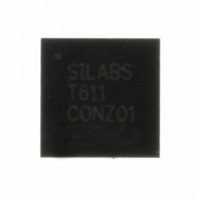
C8051T611-GM Silicon Laboratories Inc, C8051T611-GM Datasheet - Page 94

C8051T611-GM
Manufacturer Part Number
C8051T611-GM
Description
IC 8051 MCU 16K BYTE-PROG 28-QFN
Manufacturer
Silicon Laboratories Inc
Series
C8051T61xr
Specifications of C8051T611-GM
Core Processor
8051
Core Size
8-Bit
Speed
25MHz
Connectivity
SMBus (2-Wire/I²C), SPI, UART/USART
Peripherals
POR, PWM, Temp Sensor, WDT
Number Of I /o
25
Program Memory Size
16KB (16K x 8)
Program Memory Type
OTP
Ram Size
1.25K x 8
Voltage - Supply (vcc/vdd)
1.8 V ~ 3.6 V
Data Converters
A/D 17x10b
Oscillator Type
Internal
Operating Temperature
-40°C ~ 85°C
Package / Case
28-QFN
Processor Series
C8051T6x
Core
8051
Data Bus Width
8 bit
Data Ram Size
1.25 KB
Interface Type
I2C, SPI, UART
Maximum Clock Frequency
25 MHz
Number Of Programmable I/os
29
Number Of Timers
4
Maximum Operating Temperature
+ 85 C
Mounting Style
SMD/SMT
3rd Party Development Tools
PK51, CA51, A51, ULINK2
Development Tools By Supplier
C8051FT610DK
Minimum Operating Temperature
- 40 C
On-chip Adc
10 bit, 21 Channel
Lead Free Status / RoHS Status
Lead free / RoHS Compliant
Eeprom Size
-
Lead Free Status / Rohs Status
Details
Other names
336-1436-5
Available stocks
Company
Part Number
Manufacturer
Quantity
Price
Company:
Part Number:
C8051T611-GM
Manufacturer:
Silicon Labs
Quantity:
135
Company:
Part Number:
C8051T611-GMR
Manufacturer:
SILICON
Quantity:
3 500
Part Number:
C8051T611-GMR
Manufacturer:
SILICON LABS/芯科
Quantity:
20 000
C8051T610/1/2/3/4/5/6/7
17. EPROM Memory
Electrically programmable read-only memory (EPROM) is included on-chip for program code storage. The
EPROM memory can be programmed via the C2 debug and programming interface when a special pro-
gramming voltage is applied to the V
pin. Each location in EPROM memory is programmable only once
PP
(i.e., non-erasable). Table 7.6 on page 34 shows the EPROM specifications.
17.1. Programming and Reading the EPROM Memory
Reading and writing the EPROM memory is accomplished through the C2 programming and debug inter-
face. When creating hardware to program the EPROM, it is necessary to follow the programming steps
listed below. Refer to the “C2 Interface Specification” available at http://www.silabs.com for details on com-
municating via the C2 interface. Section “27. C2 Interface” on page 208 has information about C2 register
addresses for the C8051T610/1/2/3/4/5/6/7.
17.1.1. EPROM Write Procedure
1. Reset the device using the RST pin.
2. Wait at least 20 µs before sending the first C2 command.
3. Place the device in core reset: Write 0x04 to the DEVCTL register.
4. Set the device to program mode (1st step): Write 0x40 to the EPCTL register.
5. Set the device to program mode (2nd step): Write 0x58 to the EPCTL register.
6. Apply the VPP programming Voltage.
7. Write the first EPROM address for programming to EPADDRH and EPADDRL.
8. Write a data byte to EPDAT. EPADDRH:L will increment by 1 after this write.
9. Use a C2 Address Read command to poll for write completion.
10.(Optional) Check the ERROR bit in register EPSTAT and abort the programming operation if necessary.
11. If programming is not finished, return to Step 8 to write the next address in sequence, or return to
Step 7 to program a new address.
12.Remove the VPP programming Voltage.
13.Remove program mode (1st step): Write 0x40 to the EPCTL register.
14.Remove program mode (2nd step): Write 0x00 to the EPCTL register.
15.Reset the device: Write 0x02 and then 0x00 to the DEVCTL register.
Important Note: There is a finite amount of time which V
can be applied without damaging the device,
PP
which is cumulative over the life of the device. Refer to Table 7.1 on page 31 for the V
timing specifica-
PP
tion.
94
Rev 1.0


