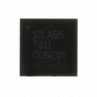
C8051T611-GM Silicon Laboratories Inc, C8051T611-GM Datasheet - Page 116

C8051T611-GM
Manufacturer Part Number
C8051T611-GM
Description
IC 8051 MCU 16K BYTE-PROG 28-QFN
Manufacturer
Silicon Laboratories Inc
Series
C8051T61xr
Specifications of C8051T611-GM
Core Processor
8051
Core Size
8-Bit
Speed
25MHz
Connectivity
SMBus (2-Wire/I²C), SPI, UART/USART
Peripherals
POR, PWM, Temp Sensor, WDT
Number Of I /o
25
Program Memory Size
16KB (16K x 8)
Program Memory Type
OTP
Ram Size
1.25K x 8
Voltage - Supply (vcc/vdd)
1.8 V ~ 3.6 V
Data Converters
A/D 17x10b
Oscillator Type
Internal
Operating Temperature
-40°C ~ 85°C
Package / Case
28-QFN
Processor Series
C8051T6x
Core
8051
Data Bus Width
8 bit
Data Ram Size
1.25 KB
Interface Type
I2C, SPI, UART
Maximum Clock Frequency
25 MHz
Number Of Programmable I/os
29
Number Of Timers
4
Maximum Operating Temperature
+ 85 C
Mounting Style
SMD/SMT
3rd Party Development Tools
PK51, CA51, A51, ULINK2
Development Tools By Supplier
C8051FT610DK
Minimum Operating Temperature
- 40 C
On-chip Adc
10 bit, 21 Channel
Lead Free Status / RoHS Status
Lead free / RoHS Compliant
Eeprom Size
-
Lead Free Status / Rohs Status
Details
Other names
336-1436-5
Available stocks
Company
Part Number
Manufacturer
Quantity
Price
Company:
Part Number:
C8051T611-GM
Manufacturer:
Silicon Labs
Quantity:
135
Company:
Part Number:
C8051T611-GMR
Manufacturer:
SILICON
Quantity:
3 500
Part Number:
C8051T611-GMR
Manufacturer:
SILICON LABS/芯科
Quantity:
20 000
C8051T610/1/2/3/4/5/6/7
21.2. Assigning Port I/O Pins to Analog and Digital Functions
Port I/O pins can be assigned to various analog, digital, and external interrupt functions. The Port pins
assigned to analog functions should be configured for analog I/O, and Port pins assigned to digital or exter-
nal interrupt functions should be configured for digital I/O.
21.2.1. Assigning Port I/O Pins to Analog Functions
Table 21.1 shows all available analog functions that require Port I/O assignments. Port pins selected for
these analog functions should have their corresponding bit in PnSKIP set to 1. This reserves the pin
for use by the analog function and does not allow it to be claimed by the Crossbar. Table 21.1 shows the
potential mapping of Port I/O to each analog function.
21.2.2. Assigning Port I/O Pins to Digital Functions
Any Port pins not assigned to analog functions may be assigned to digital functions or used as GPIO. Most
digital functions rely on the Crossbar for pin assignment; however, some digital functions bypass the
Crossbar in a manner similar to the analog functions listed above. Port pins used by these digital func-
tions and any Port pins selected for use as GPIO should have their corresponding bit in PnSKIP set
to 1. Table 21.2 shows all available digital functions and the potential mapping of Port I/O to each digital
function.
116
Analog Function
ADC Input
Comparator Inputs
Voltage Reference (VREF0)
External Oscillator in RC or C Mode (EXTCLK)
Digital Function
UART0, SPI0, SMBus, CP0,
CP0A, CP1, CP1A,
SYSCLK, PCA0 (CEX0-4
and ECI), T0 or T1.
Any pin used for GPIO
Table 21.1. Port I/O Assignment for Analog Functions
Table 21.2. Port I/O Assignment for Digital Functions
Any Port pin available for assignment by the
Crossbar. This includes P0.0 - P2.3 pins which
have their PnSKIP bit set to 0.
Note: The Crossbar will always assign UART0
pins to P0.4 and P0.5.
Potentially Assignable Port Pins
Rev 1.0
P0.0–P3.4
Potentially Assignable
P1.0–P3.4
P1.0–P2.7
Port Pins
P0.0
P0.3
CPT0MX, CPT1MX,
OSCXCN, PnSKIP
REF0CN, PnSKIP
SFR(s) used for
SFR(s) used for
AMX0P, PnSKIP
Assignment
XBR0, XBR1
Assignment
PnSKIP
PnSKIP


