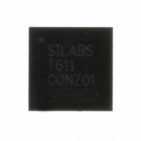
C8051T611-GM Silicon Laboratories Inc, C8051T611-GM Datasheet - Page 42

C8051T611-GM
Manufacturer Part Number
C8051T611-GM
Description
IC 8051 MCU 16K BYTE-PROG 28-QFN
Manufacturer
Silicon Laboratories Inc
Series
C8051T61xr
Specifications of C8051T611-GM
Core Processor
8051
Core Size
8-Bit
Speed
25MHz
Connectivity
SMBus (2-Wire/I²C), SPI, UART/USART
Peripherals
POR, PWM, Temp Sensor, WDT
Number Of I /o
25
Program Memory Size
16KB (16K x 8)
Program Memory Type
OTP
Ram Size
1.25K x 8
Voltage - Supply (vcc/vdd)
1.8 V ~ 3.6 V
Data Converters
A/D 17x10b
Oscillator Type
Internal
Operating Temperature
-40°C ~ 85°C
Package / Case
28-QFN
Processor Series
C8051T6x
Core
8051
Data Bus Width
8 bit
Data Ram Size
1.25 KB
Interface Type
I2C, SPI, UART
Maximum Clock Frequency
25 MHz
Number Of Programmable I/os
29
Number Of Timers
4
Maximum Operating Temperature
+ 85 C
Mounting Style
SMD/SMT
3rd Party Development Tools
PK51, CA51, A51, ULINK2
Development Tools By Supplier
C8051FT610DK
Minimum Operating Temperature
- 40 C
On-chip Adc
10 bit, 21 Channel
Lead Free Status / RoHS Status
Lead free / RoHS Compliant
Eeprom Size
-
Lead Free Status / Rohs Status
Details
Other names
336-1436-5
Available stocks
Company
Part Number
Manufacturer
Quantity
Price
Company:
Part Number:
C8051T611-GM
Manufacturer:
Silicon Labs
Quantity:
135
Company:
Part Number:
C8051T611-GMR
Manufacturer:
SILICON
Quantity:
3 500
Part Number:
C8051T611-GMR
Manufacturer:
SILICON LABS/芯科
Quantity:
20 000
C8051T610/1/2/3/4/5/6/7
8.3.3. Settling Time Requirements
A minimum tracking time is required before each conversion to ensure that an accurate conversion is per-
formed. This tracking time is determined by any series impedance, including the AMUX0 resistance, the
the ADC0 sampling capacitance, and the accuracy required for the conversion. Note that in delayed track-
ing mode, three SAR clocks are used for tracking at the start of every conversion. For many applications,
these three SAR clocks will meet the minimum tracking time requirements.
Figure 8.3 shows the equivalent ADC0 input circuit. The required ADC0 settling time for a given settling
accuracy (SA) may be approximated by Equation 8.1. See Table 7.8 for ADC0 minimum settling time
requirements as well as the mux impedance and sampling capacitor values.
Where:
SA is the settling accuracy, given as a fraction of an LSB (for example, 0.25 to settle within 1/4 LSB)
t is the required settling time in seconds
R
n is the ADC resolution in bits (10).
42
TOTAL
is the sum of the AMUX0 resistance and any external source resistance.
Note: See electrical specification tables for R
Input Pin
Equation 8.1. ADC0 Settling Time Requirements
Figure 8.3. ADC0 Equivalent Input Circuits
t
=
RC
MUX Select
ln
Input
------ -
SA
= R
2
n
MUX
* C
R
Rev 1.0
R
TOTAL
SAMPLE
MUX
C
SAMPLE
MUX
and C
C
SAMPLE
SAMPLE
parameters.


