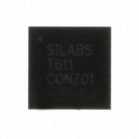
C8051T611-GM Silicon Laboratories Inc, C8051T611-GM Datasheet - Page 130

C8051T611-GM
Manufacturer Part Number
C8051T611-GM
Description
IC 8051 MCU 16K BYTE-PROG 28-QFN
Manufacturer
Silicon Laboratories Inc
Series
C8051T61xr
Specifications of C8051T611-GM
Core Processor
8051
Core Size
8-Bit
Speed
25MHz
Connectivity
SMBus (2-Wire/I²C), SPI, UART/USART
Peripherals
POR, PWM, Temp Sensor, WDT
Number Of I /o
25
Program Memory Size
16KB (16K x 8)
Program Memory Type
OTP
Ram Size
1.25K x 8
Voltage - Supply (vcc/vdd)
1.8 V ~ 3.6 V
Data Converters
A/D 17x10b
Oscillator Type
Internal
Operating Temperature
-40°C ~ 85°C
Package / Case
28-QFN
Processor Series
C8051T6x
Core
8051
Data Bus Width
8 bit
Data Ram Size
1.25 KB
Interface Type
I2C, SPI, UART
Maximum Clock Frequency
25 MHz
Number Of Programmable I/os
29
Number Of Timers
4
Maximum Operating Temperature
+ 85 C
Mounting Style
SMD/SMT
3rd Party Development Tools
PK51, CA51, A51, ULINK2
Development Tools By Supplier
C8051FT610DK
Minimum Operating Temperature
- 40 C
On-chip Adc
10 bit, 21 Channel
Lead Free Status / RoHS Status
Lead free / RoHS Compliant
Eeprom Size
-
Lead Free Status / Rohs Status
Details
Other names
336-1436-5
Available stocks
Company
Part Number
Manufacturer
Quantity
Price
Company:
Part Number:
C8051T611-GM
Manufacturer:
Silicon Labs
Quantity:
135
Company:
Part Number:
C8051T611-GMR
Manufacturer:
SILICON
Quantity:
3 500
Part Number:
C8051T611-GMR
Manufacturer:
SILICON LABS/芯科
Quantity:
20 000
C8051T610/1/2/3/4/5/6/7
SFR Definition 21.14. P2SKIP: Port 2 Skip
SFR Address = 0xD6
SFR Definition 21.15. P3: Port 3
SFR Address = 0xB0; Bit-Addressable
130
Note: Only P2.0-P2.3 are associated with the crossbar.
Note: P3.1-P3.4 are not connected to external pins on the C8051T611/3/5 and C8051T616/7 devices.
Name
Reset
Name
Reset
7:4
3:0
7:5
4:0
Bit
Bit
Type
Type
Bit
Bit
Unused
P2SKIP[3:0]
P3[4:0]
Name
Unused
Name
R
7
0
7
0
Unused. Read = 000b; Write = Don’t Care.
Port 3 Data.
Sets the Port latch logic
value or reads the Port pin
logic state in Port cells con-
figured for digital I/O.
Unused. Read = 0000b; Write = Don’t Care.
Port 2 Crossbar Skip Enable Bits.
These bits select Port 2 pins to be skipped by the Crossbar Decoder. Port pins
used for analog, special functions or GPIO should be skipped by the Crossbar.
0: Corresponding P2.n pin is not skipped by the Crossbar.
1: Corresponding P2.n pin is skipped by the Crossbar.
R
6
0
6
0
Description
R
R
5
0
5
0
0: Set output latch to logic
LOW.
1: Set output latch to logic
HIGH.
Rev 1.0
4
0
4
1
Function
Write
3
0
3
1
P3[4:0]
R/W
2
0
2
1
P2SKIP[3:0]
0: P3.n Port pin is logic
LOW.
1: P3.n Port pin is logic
HIGH.
R/W
1
0
1
1
Read
0
0
0
1


