C8051T611-GM Silicon Laboratories Inc, C8051T611-GM Datasheet - Page 45
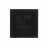
C8051T611-GM
Manufacturer Part Number
C8051T611-GM
Description
IC 8051 MCU 16K BYTE-PROG 28-QFN
Manufacturer
Silicon Laboratories Inc
Series
C8051T61xr
Specifications of C8051T611-GM
Core Processor
8051
Core Size
8-Bit
Speed
25MHz
Connectivity
SMBus (2-Wire/I²C), SPI, UART/USART
Peripherals
POR, PWM, Temp Sensor, WDT
Number Of I /o
25
Program Memory Size
16KB (16K x 8)
Program Memory Type
OTP
Ram Size
1.25K x 8
Voltage - Supply (vcc/vdd)
1.8 V ~ 3.6 V
Data Converters
A/D 17x10b
Oscillator Type
Internal
Operating Temperature
-40°C ~ 85°C
Package / Case
28-QFN
Processor Series
C8051T6x
Core
8051
Data Bus Width
8 bit
Data Ram Size
1.25 KB
Interface Type
I2C, SPI, UART
Maximum Clock Frequency
25 MHz
Number Of Programmable I/os
29
Number Of Timers
4
Maximum Operating Temperature
+ 85 C
Mounting Style
SMD/SMT
3rd Party Development Tools
PK51, CA51, A51, ULINK2
Development Tools By Supplier
C8051FT610DK
Minimum Operating Temperature
- 40 C
On-chip Adc
10 bit, 21 Channel
Lead Free Status / RoHS Status
Lead free / RoHS Compliant
Eeprom Size
-
Lead Free Status / Rohs Status
Details
Other names
336-1436-5
Available stocks
Company
Part Number
Manufacturer
Quantity
Price
Company:

Part Number:
C8051T611-GM
Manufacturer:
Silicon Labs
Quantity:
135
Company:
Part Number:
C8051T611-GMR
Manufacturer:
SILICON
Quantity:
3 500
Part Number:
C8051T611-GMR
Manufacturer:
SILICON LABS/芯科
Quantity:
20 000


SFR Definition 8.4. ADC0CN: ADC0 Control
SFR Address = 0xE8; Bit-Addressable
Name
Reset
Bit
2:0 AD0CM[2:0] ADC0 Start of Conversion Mode Select.
Type
7
6
5
4
3
Bit
AD0BUSY ADC0 Busy Bit.
AD0WINT
AD0INT
AD0EN
AD0TM
Name
AD0EN
R/W
7
0
ADC0 Enable Bit.
0: ADC0 Disabled. ADC0 is in low-power shutdown.
1: ADC0 Enabled. ADC0 is active and ready for data conversions.
ADC0 Track Mode Bit.
0: Normal Track Mode: When ADC0 is enabled, tracking is continuous unless a con-
version is in progress. Conversion begins immediately on start-of-conversion event,
as defined by AD0CM[2:0].
1: Delayed Track Mode: When ADC0 is enabled, input is tracked when a conversion
is not in progress. A start-of-conversion signal initiates three SAR clocks of additional
tracking, and then begins the conversion.
ADC0 Conversion Complete Interrupt Flag.
0: ADC0 has not completed a data conversion since AD0INT was last cleared.
1: ADC0 has completed a data conversion.
ADC0 Window Compare Interrupt Flag.
0: ADC0 Window Comparison Data match has not occurred since this flag was last
cleared.
1: ADC0 Window Comparison Data match has occurred.
000: ADC0 start-of-conversion source is write of 1 to AD0BUSY.
001: ADC0 start-of-conversion source is overflow of Timer 0.
010: ADC0 start-of-conversion source is overflow of Timer 2.
011: ADC0 start-of-conversion source is overflow of Timer 1.
100: ADC0 start-of-conversion source is rising edge of external CNVSTR.
101: ADC0 start-of-conversion source is overflow of Timer 3.
11x: Reserved.
AD0TM
R/W
6
0
AD0INT
R/W
5
0
Read:
0: ADC0 conversion is not in
progress.
1: ADC0 conversion is in prog-
ress.
AD0BUSY AD0WINT
R/W
Rev 1.0
4
0
C8051T610/1/2/3/4/5/6/7
Function
R/W
3
0
Write:
0: No Effect.
1: Initiates ADC0 Conversion if
AD0CM[2:0] = 000b
2
0
AD0CM[2:0]
R/W
1
0
0
0
45
Related parts for C8051T611-GM
Image
Part Number
Description
Manufacturer
Datasheet
Request
R

Part Number:
Description:
SMD/C°/SINGLE-ENDED OUTPUT SILICON OSCILLATOR
Manufacturer:
Silicon Laboratories Inc
Part Number:
Description:
Manufacturer:
Silicon Laboratories Inc
Datasheet:
Part Number:
Description:
N/A N/A/SI4010 AES KEYFOB DEMO WITH LCD RX
Manufacturer:
Silicon Laboratories Inc
Datasheet:
Part Number:
Description:
N/A N/A/SI4010 SIMPLIFIED KEY FOB DEMO WITH LED RX
Manufacturer:
Silicon Laboratories Inc
Datasheet:
Part Number:
Description:
N/A/-40 TO 85 OC/EZLINK MODULE; F930/4432 HIGH BAND (REV E/B1)
Manufacturer:
Silicon Laboratories Inc
Part Number:
Description:
EZLink Module; F930/4432 Low Band (rev e/B1)
Manufacturer:
Silicon Laboratories Inc
Part Number:
Description:
I°/4460 10 DBM RADIO TEST CARD 434 MHZ
Manufacturer:
Silicon Laboratories Inc
Part Number:
Description:
I°/4461 14 DBM RADIO TEST CARD 868 MHZ
Manufacturer:
Silicon Laboratories Inc
Part Number:
Description:
I°/4463 20 DBM RFSWITCH RADIO TEST CARD 460 MHZ
Manufacturer:
Silicon Laboratories Inc
Part Number:
Description:
I°/4463 20 DBM RADIO TEST CARD 868 MHZ
Manufacturer:
Silicon Laboratories Inc
Part Number:
Description:
I°/4463 27 DBM RADIO TEST CARD 868 MHZ
Manufacturer:
Silicon Laboratories Inc
Part Number:
Description:
I°/4463 SKYWORKS 30 DBM RADIO TEST CARD 915 MHZ
Manufacturer:
Silicon Laboratories Inc
Part Number:
Description:
N/A N/A/-40 TO 85 OC/4463 RFMD 30 DBM RADIO TEST CARD 915 MHZ
Manufacturer:
Silicon Laboratories Inc
Part Number:
Description:
I°/4463 20 DBM RADIO TEST CARD 169 MHZ
Manufacturer:
Silicon Laboratories Inc