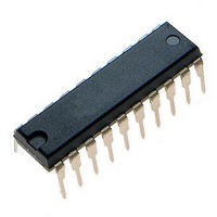
MCR908JK1ECPE Freescale Semiconductor, MCR908JK1ECPE Datasheet - Page 163

MCR908JK1ECPE
Manufacturer Part Number
MCR908JK1ECPE
Description
IC MCU 1.5K FLASH 8MHZ 20-DIP
Manufacturer
Freescale Semiconductor
Series
HC08r
Datasheet
1.MC908JK1ECDWE.pdf
(180 pages)
Specifications of MCR908JK1ECPE
Core Processor
HC08
Core Size
8-Bit
Speed
8MHz
Peripherals
LED, LVD, POR, PWM
Number Of I /o
14
Program Memory Size
1.5KB (1.5K x 8)
Program Memory Type
FLASH
Ram Size
128 x 8
Voltage - Supply (vcc/vdd)
2.7 V ~ 3.3 V
Data Converters
A/D 12x8b
Oscillator Type
External
Operating Temperature
-40°C ~ 85°C
Package / Case
20-DIP (0.300", 7.62mm)
Processor Series
HC08JK
Core
HC08
Data Bus Width
8 bit
Data Ram Size
128 B
Maximum Clock Frequency
8 MHz
Number Of Programmable I/os
15
Number Of Timers
2
Maximum Operating Temperature
+ 85 C
Mounting Style
Through Hole
Development Tools By Supplier
FSICEBASE, DEMO908JL16E, M68CBL05CE
Minimum Operating Temperature
- 40 C
On-chip Adc
8 bit, 12 Channel
Lead Free Status / RoHS Status
Lead free / RoHS Compliant
Eeprom Size
-
Connectivity
-
Lead Free Status / Rohs Status
Details
Available stocks
Company
Part Number
Manufacturer
Quantity
Price
Company:
Part Number:
MCR908JK1ECPE
Manufacturer:
Freescale Semiconductor
Quantity:
135
A.5.6 Memory Characteristics
The Flash memory can only be read at an operating voltage of 2.2 to 5.5V. Program and erase are
achieved at an operating voltage of 2.7 to 5.5V. The program and erase parameters in
V
Freescale Semiconductor
RAM data retention voltage
Flash program bus clock frequency
Flash read bus clock frequency
Flash page erase time
Flash mass erase time
Flash PGM/ERASE to HVEN set up time
Flash high-voltage hold time
Flash high-voltage hold time (mass erase)
Flash program hold time
Flash program time
Flash return to read time
Flash cumulative program hv period
Flash row erase endurance
Flash row program endurance
Flash data retention time
DD
1. f
2. If the page erase time is longer than t
3. If the mass erase time is longer than t
4. t
5. t
6. The minimum row endurance value specifies each row of the Flash memory is guaranteed to work for at least this many
7. The minimum row endurance value specifies each row of the Flash memory is guaranteed to work for at least this many
8. The Flash is guaranteed to retain data over the entire operating temperature range for at least the minimum time specified.
ory.
memory.
HVEN to 0.
t
erase / program cycles.
erase / program cycles.
Read
rcv
HV
HV
= 2.7 to 5.5V only.
is defined as the time it needs before the Flash can be read after turning off the high voltage charge pump, by clearing
is defined as the cumulative high voltage programming time to the same row before next erase.
must satisfy this condition: t
is defined as the frequency range for which the Flash memory can be read.
(8)
(6)
Characteristic
(7)
nvs
+ t
MC68HC908JL3E Family Data Sheet, Rev. 4
Table A-6. Memory Characteristics
Erase
nvh
MErase
+ t
(Min), there is no erase-disturb, but it reduces the endurance of the Flash mem-
pgs
(Min), there is no erase-disturb, but it reduces the endurance of the Flash
+ (t
PROG
× 32) ≤ t
HV
max.
t
Symbol
MErase
t
f
Erase
Read
t
V
t
t
PROG
HV
t
rcv
t
t
t
nvhl
RDR
pgs
—
nvs
nvh
—
—
—
(4)
(5)
(1)
(2)
(3)
Min
32k
100
10k
10k
1.3
10
30
—
10
1
1
4
5
5
1
Table A-6
Max
8M
40
—
—
—
—
—
—
—
—
—
—
—
—
4
cycles
cycles
years
MHz
Unit
are for
ms
ms
ms
Hz
μs
μs
μs
μs
μs
μs
V
163


