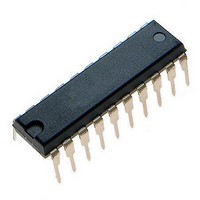
MCR908JK1ECPE Freescale Semiconductor, MCR908JK1ECPE Datasheet - Page 81

MCR908JK1ECPE
Manufacturer Part Number
MCR908JK1ECPE
Description
IC MCU 1.5K FLASH 8MHZ 20-DIP
Manufacturer
Freescale Semiconductor
Series
HC08r
Datasheet
1.MC908JK1ECDWE.pdf
(180 pages)
Specifications of MCR908JK1ECPE
Core Processor
HC08
Core Size
8-Bit
Speed
8MHz
Peripherals
LED, LVD, POR, PWM
Number Of I /o
14
Program Memory Size
1.5KB (1.5K x 8)
Program Memory Type
FLASH
Ram Size
128 x 8
Voltage - Supply (vcc/vdd)
2.7 V ~ 3.3 V
Data Converters
A/D 12x8b
Oscillator Type
External
Operating Temperature
-40°C ~ 85°C
Package / Case
20-DIP (0.300", 7.62mm)
Processor Series
HC08JK
Core
HC08
Data Bus Width
8 bit
Data Ram Size
128 B
Maximum Clock Frequency
8 MHz
Number Of Programmable I/os
15
Number Of Timers
2
Maximum Operating Temperature
+ 85 C
Mounting Style
Through Hole
Development Tools By Supplier
FSICEBASE, DEMO908JL16E, M68CBL05CE
Minimum Operating Temperature
- 40 C
On-chip Adc
8 bit, 12 Channel
Lead Free Status / RoHS Status
Lead free / RoHS Compliant
Eeprom Size
-
Connectivity
-
Lead Free Status / Rohs Status
Details
Available stocks
Company
Part Number
Manufacturer
Quantity
Price
Company:
Part Number:
MCR908JK1ECPE
Manufacturer:
Freescale Semiconductor
Quantity:
135
- Current page: 81 of 180
- Download datasheet (3Mb)
Chapter 8
Timer Interface Module (TIM)
8.1 Introduction
This section describes the timer interface module (TIM2, Version B). The TIM is a two-channel timer that
provides a timing reference with input capture, output compare, and pulse-width-modulation functions.
Figure 8-1
8.2 Features
Features of the TIM include the following:
8.3 Pin Name Conventions
The TIM share two I/O pins with two port D I/O pins. The full name of the TIM I/O pins are listed in
Table
Freescale Semiconductor
•
•
•
•
•
•
8-1. The generic pin name appear in the text that follows.
Two input capture/output compare channels
–
–
Buffered and unbuffered pulse width modulation (PWM) signal generation
Programmable TIM clock input with 7-frequency internal bus clock prescaler selection
Free-running or modulo up-count operation
Toggle any channel pin on overflow
TIM counter stop and reset bits
Rising-edge, falling-edge, or any-edge input capture trigger
Set, clear, or toggle output compare action
is a block diagram of the TIM.
TIM Generic Pin Names:
Full TIM Pin Names:
MC68HC908JL3E Family Data Sheet, Rev. 4
Table 8-1. Pin Name Conventions
PTD4/TCH0
TCH0
PTD5/TCH1
TCH1
81
Related parts for MCR908JK1ECPE
Image
Part Number
Description
Manufacturer
Datasheet
Request
R
Part Number:
Description:
Manufacturer:
Freescale Semiconductor, Inc
Datasheet:
Part Number:
Description:
Manufacturer:
Freescale Semiconductor, Inc
Datasheet:
Part Number:
Description:
Manufacturer:
Freescale Semiconductor, Inc
Datasheet:
Part Number:
Description:
Manufacturer:
Freescale Semiconductor, Inc
Datasheet:
Part Number:
Description:
Manufacturer:
Freescale Semiconductor, Inc
Datasheet:
Part Number:
Description:
Manufacturer:
Freescale Semiconductor, Inc
Datasheet:
Part Number:
Description:
Manufacturer:
Freescale Semiconductor, Inc
Datasheet:
Part Number:
Description:
Manufacturer:
Freescale Semiconductor, Inc
Datasheet:
Part Number:
Description:
Manufacturer:
Freescale Semiconductor, Inc
Datasheet:
Part Number:
Description:
Manufacturer:
Freescale Semiconductor, Inc
Datasheet:
Part Number:
Description:
Manufacturer:
Freescale Semiconductor, Inc
Datasheet:
Part Number:
Description:
Manufacturer:
Freescale Semiconductor, Inc
Datasheet:
Part Number:
Description:
Manufacturer:
Freescale Semiconductor, Inc
Datasheet:
Part Number:
Description:
Manufacturer:
Freescale Semiconductor, Inc
Datasheet:
Part Number:
Description:
Manufacturer:
Freescale Semiconductor, Inc
Datasheet:


