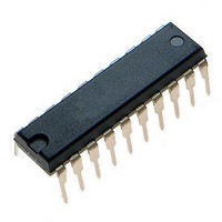
MCR908JK1ECPE Freescale Semiconductor, MCR908JK1ECPE Datasheet - Page 29

MCR908JK1ECPE
Manufacturer Part Number
MCR908JK1ECPE
Description
IC MCU 1.5K FLASH 8MHZ 20-DIP
Manufacturer
Freescale Semiconductor
Series
HC08r
Datasheet
1.MC908JK1ECDWE.pdf
(180 pages)
Specifications of MCR908JK1ECPE
Core Processor
HC08
Core Size
8-Bit
Speed
8MHz
Peripherals
LED, LVD, POR, PWM
Number Of I /o
14
Program Memory Size
1.5KB (1.5K x 8)
Program Memory Type
FLASH
Ram Size
128 x 8
Voltage - Supply (vcc/vdd)
2.7 V ~ 3.3 V
Data Converters
A/D 12x8b
Oscillator Type
External
Operating Temperature
-40°C ~ 85°C
Package / Case
20-DIP (0.300", 7.62mm)
Processor Series
HC08JK
Core
HC08
Data Bus Width
8 bit
Data Ram Size
128 B
Maximum Clock Frequency
8 MHz
Number Of Programmable I/os
15
Number Of Timers
2
Maximum Operating Temperature
+ 85 C
Mounting Style
Through Hole
Development Tools By Supplier
FSICEBASE, DEMO908JL16E, M68CBL05CE
Minimum Operating Temperature
- 40 C
On-chip Adc
8 bit, 12 Channel
Lead Free Status / RoHS Status
Lead free / RoHS Compliant
Eeprom Size
-
Connectivity
-
Lead Free Status / Rohs Status
Details
Available stocks
Company
Part Number
Manufacturer
Quantity
Price
Company:
Part Number:
MCR908JK1ECPE
Manufacturer:
Freescale Semiconductor
Quantity:
135
- Current page: 29 of 180
- Download datasheet (3Mb)
2.7 Flash Control Register
The Flash Control Register controls Flash program and erase operations.
HVEN — High Voltage Enable Bit
MASS — Mass Erase Control Bit
ERASE — Erase Control Bit
PGM — Program Control Bit
Freescale Semiconductor
This read/write bit enables high voltage from the charge pump to the memory for either program or
erase operation. It can only be set if either PGM=1 or ERASE=1 and the proper sequence for program
or erase is followed.
This read/write bit configures the memory for mass erase operation or page erase operation when the
ERASE bit is set.
This read/write bit configures the memory for erase operation. This bit and the PGM bit should not be
set to 1 at the same time.
This read/write bit configures the memory for program operation. This bit and the ERASE bit should
not be set to 1 at the same time.
1 = High voltage enabled to array and charge pump on
0 = High voltage disabled to array and charge pump off
1 = Mass erase operation selected
0 = Page erase operation selected
1 = Erase operation selected
0 = Erase operation not selected
1 = Program operation selected
0 = Program operation not selected
Address:
Reset:
Read:
Write:
$FE08
Bit 7
0
0
Figure 2-4. Flash Control Register (FLCR)
= Unimplemented
MC68HC908JL3E Family Data Sheet, Rev. 4
6
0
0
5
0
0
4
0
0
HVEN
3
0
MASS
2
0
ERASE
1
0
Flash Control Register
PGM
Bit 0
0
29
Related parts for MCR908JK1ECPE
Image
Part Number
Description
Manufacturer
Datasheet
Request
R
Part Number:
Description:
Manufacturer:
Freescale Semiconductor, Inc
Datasheet:
Part Number:
Description:
Manufacturer:
Freescale Semiconductor, Inc
Datasheet:
Part Number:
Description:
Manufacturer:
Freescale Semiconductor, Inc
Datasheet:
Part Number:
Description:
Manufacturer:
Freescale Semiconductor, Inc
Datasheet:
Part Number:
Description:
Manufacturer:
Freescale Semiconductor, Inc
Datasheet:
Part Number:
Description:
Manufacturer:
Freescale Semiconductor, Inc
Datasheet:
Part Number:
Description:
Manufacturer:
Freescale Semiconductor, Inc
Datasheet:
Part Number:
Description:
Manufacturer:
Freescale Semiconductor, Inc
Datasheet:
Part Number:
Description:
Manufacturer:
Freescale Semiconductor, Inc
Datasheet:
Part Number:
Description:
Manufacturer:
Freescale Semiconductor, Inc
Datasheet:
Part Number:
Description:
Manufacturer:
Freescale Semiconductor, Inc
Datasheet:
Part Number:
Description:
Manufacturer:
Freescale Semiconductor, Inc
Datasheet:
Part Number:
Description:
Manufacturer:
Freescale Semiconductor, Inc
Datasheet:
Part Number:
Description:
Manufacturer:
Freescale Semiconductor, Inc
Datasheet:
Part Number:
Description:
Manufacturer:
Freescale Semiconductor, Inc
Datasheet:


