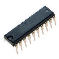
MCR908JK1ECPE Freescale Semiconductor, MCR908JK1ECPE Datasheet - Page 28

MCR908JK1ECPE
Manufacturer Part Number
MCR908JK1ECPE
Description
IC MCU 1.5K FLASH 8MHZ 20-DIP
Manufacturer
Freescale Semiconductor
Series
HC08r
Datasheet
1.MC908JK1ECDWE.pdf
(180 pages)
Specifications of MCR908JK1ECPE
Core Processor
HC08
Core Size
8-Bit
Speed
8MHz
Peripherals
LED, LVD, POR, PWM
Number Of I /o
14
Program Memory Size
1.5KB (1.5K x 8)
Program Memory Type
FLASH
Ram Size
128 x 8
Voltage - Supply (vcc/vdd)
2.7 V ~ 3.3 V
Data Converters
A/D 12x8b
Oscillator Type
External
Operating Temperature
-40°C ~ 85°C
Package / Case
20-DIP (0.300", 7.62mm)
Processor Series
HC08JK
Core
HC08
Data Bus Width
8 bit
Data Ram Size
128 B
Maximum Clock Frequency
8 MHz
Number Of Programmable I/os
15
Number Of Timers
2
Maximum Operating Temperature
+ 85 C
Mounting Style
Through Hole
Development Tools By Supplier
FSICEBASE, DEMO908JL16E, M68CBL05CE
Minimum Operating Temperature
- 40 C
On-chip Adc
8 bit, 12 Channel
Lead Free Status / RoHS Status
Lead free / RoHS Compliant
Eeprom Size
-
Connectivity
-
Lead Free Status / Rohs Status
Details
Available stocks
Company
Part Number
Manufacturer
Quantity
Price
Company:
Part Number:
MCR908JK1ECPE
Manufacturer:
Freescale Semiconductor
Quantity:
135
- Current page: 28 of 180
- Download datasheet (3Mb)
Memory
During a subroutine call, the CPU uses two bytes of the stack to store the return address. The stack
pointer decrements during pushes and increments during pulls.
2.5 Flash Memory
This sub-section describes the operation of the embedded Flash memory. The Flash memory can be
read, programmed, and erased from a single external supply. The program and erase operations are
enabled through the use of an internal charge pump.
2.6 Functional Description
The Flash memory consists of an array of 4,096 or 1,536 bytes with an additional 48 bytes for user
vectors. The minimum size of Flash memory that can be erased is 64 bytes (a page); and the maximum
size of Flash memory that can be programmed in a program cycle is 32 bytes (a row). Program and erase
operations are facilitated through control bits in the Flash Control Register (FLCR). Details for these
operations appear later in this section. The address ranges for the user memory and vectors are:
1. No security feature is absolutely secure. However, Freescale’s strategy is to make reading or copying the Flash difficult for
28
Addr.
$FE08
$FE09
unauthorized users.
•
•
$EC00–$FBFF; user memory; 4,096 bytes; MC68H(R)C908JL3E/JK3E
$F600–$FBFF; user memory; 1,536 bytes; MC68H(R)C908JK1E
$FFD0–$FFFF; user interrupt vectors; 48 bytes
Register Name
Flash Control Register
Flash Block Protect
Be careful when using nested subroutines. The CPU may overwrite data in
the RAM during a subroutine or during the interrupt stacking operation.
An erased bit reads as 1 and a programmed bit reads as 0. A security
feature prevents viewing of the Flash contents.
MC68H(R)C908JK3E
MC68H(R)C908JK1E
MC68H(R)C908JL3E
(FLBPR)
Register
(FLCR)
Device
Reset:
Reset:
Read:
Read:
Write:
Write:
Figure 2-3. Flash I/O Register Summary
MC68HC908JL3E Family Data Sheet, Rev. 4
BPR7
Bit 7
0
0
0
= Unimplemented
Flash Memory Size
BPR6
6
0
0
0
NOTE
(Bytes)
NOTE
4,096
4,096
1,536
BPR5
5
0
0
0
(1)
BPR4
4
0
0
0
Memory Address Range
HVEN
BPR3
$EC00—$FBFF
$EC00—$FBFF
$F600—$FBFF
3
0
0
MASS
BPR2
2
0
0
Freescale Semiconductor
ERASE
BPR1
1
0
0
BPR0
PGM
Bit 0
0
0
Related parts for MCR908JK1ECPE
Image
Part Number
Description
Manufacturer
Datasheet
Request
R
Part Number:
Description:
Manufacturer:
Freescale Semiconductor, Inc
Datasheet:
Part Number:
Description:
Manufacturer:
Freescale Semiconductor, Inc
Datasheet:
Part Number:
Description:
Manufacturer:
Freescale Semiconductor, Inc
Datasheet:
Part Number:
Description:
Manufacturer:
Freescale Semiconductor, Inc
Datasheet:
Part Number:
Description:
Manufacturer:
Freescale Semiconductor, Inc
Datasheet:
Part Number:
Description:
Manufacturer:
Freescale Semiconductor, Inc
Datasheet:
Part Number:
Description:
Manufacturer:
Freescale Semiconductor, Inc
Datasheet:
Part Number:
Description:
Manufacturer:
Freescale Semiconductor, Inc
Datasheet:
Part Number:
Description:
Manufacturer:
Freescale Semiconductor, Inc
Datasheet:
Part Number:
Description:
Manufacturer:
Freescale Semiconductor, Inc
Datasheet:
Part Number:
Description:
Manufacturer:
Freescale Semiconductor, Inc
Datasheet:
Part Number:
Description:
Manufacturer:
Freescale Semiconductor, Inc
Datasheet:
Part Number:
Description:
Manufacturer:
Freescale Semiconductor, Inc
Datasheet:
Part Number:
Description:
Manufacturer:
Freescale Semiconductor, Inc
Datasheet:
Part Number:
Description:
Manufacturer:
Freescale Semiconductor, Inc
Datasheet:


