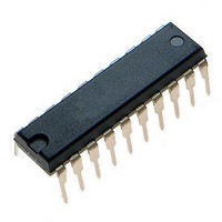
MCR908JK1ECPE Freescale Semiconductor, MCR908JK1ECPE Datasheet - Page 168

MCR908JK1ECPE
Manufacturer Part Number
MCR908JK1ECPE
Description
IC MCU 1.5K FLASH 8MHZ 20-DIP
Manufacturer
Freescale Semiconductor
Series
HC08r
Datasheet
1.MC908JK1ECDWE.pdf
(180 pages)
Specifications of MCR908JK1ECPE
Core Processor
HC08
Core Size
8-Bit
Speed
8MHz
Peripherals
LED, LVD, POR, PWM
Number Of I /o
14
Program Memory Size
1.5KB (1.5K x 8)
Program Memory Type
FLASH
Ram Size
128 x 8
Voltage - Supply (vcc/vdd)
2.7 V ~ 3.3 V
Data Converters
A/D 12x8b
Oscillator Type
External
Operating Temperature
-40°C ~ 85°C
Package / Case
20-DIP (0.300", 7.62mm)
Processor Series
HC08JK
Core
HC08
Data Bus Width
8 bit
Data Ram Size
128 B
Maximum Clock Frequency
8 MHz
Number Of Programmable I/os
15
Number Of Timers
2
Maximum Operating Temperature
+ 85 C
Mounting Style
Through Hole
Development Tools By Supplier
FSICEBASE, DEMO908JL16E, M68CBL05CE
Minimum Operating Temperature
- 40 C
On-chip Adc
8 bit, 12 Channel
Lead Free Status / RoHS Status
Lead free / RoHS Compliant
Eeprom Size
-
Connectivity
-
Lead Free Status / Rohs Status
Details
Available stocks
Company
Part Number
Manufacturer
Quantity
Price
Company:
Part Number:
MCR908JK1ECPE
Manufacturer:
Freescale Semiconductor
Quantity:
135
- Current page: 168 of 180
- Download datasheet (3Mb)
B.4 Reserved Registers
The two registers at $FE08 and $FE09 are reserved locations on the MC68H(R)C08JL3E/JK3E.
On the MC68H(R)C908JL3E/JK3E, these two locations are the Flash control register and the Flash block
protect register respectively.
B.5 Mask Option Registers
This section describes the mask option registers (MOR1 and MOR2). The mask option registers enable
or disable the following options:
B.5.1 Functional Description
The mask options are hard-wired connections, specified at the same time as the ROM code, which allow
the user to customize the MCU.
B.5.2 Mask Option Register 1 (MOR1)
COPRS — COP reset period selection bit
LVID — Low Voltage Inhibit Disable Bit
168
•
•
•
•
•
•
1 = COP reset cycle is 8176 × 2OSCOUT
0 = COP reset cycle is 262,128 × 2OSCOUT
1 = Low Voltage Inhibit disabled
0 = Low Voltage Inhibit enabled
Stop mode recovery time (32 × 2OSCOUT cycles or 4096 × 2OSCOUT cycles)
STOP instruction
Computer operating properly module (COP)
COP reset period (COPRS), 8176 × 2OSCOUT or 262,128 × 2OSCOUT
Enable LVI circuit
Select LVI trip voltage
Address:
Reset:
Read:
Write:
COPRS
$001F
Bit 7
0
Figure 18-1. Mask Option Register 1 (MOR1)
= Unimplemented
MC68HC908JL3E Family Data Sheet, Rev. 4
6
0
0
5
0
0
LVID
4
0
3
0
0
SSREC
2
0
STOP
1
0
Freescale Semiconductor
COPD
Bit 0
0
Related parts for MCR908JK1ECPE
Image
Part Number
Description
Manufacturer
Datasheet
Request
R
Part Number:
Description:
Manufacturer:
Freescale Semiconductor, Inc
Datasheet:
Part Number:
Description:
Manufacturer:
Freescale Semiconductor, Inc
Datasheet:
Part Number:
Description:
Manufacturer:
Freescale Semiconductor, Inc
Datasheet:
Part Number:
Description:
Manufacturer:
Freescale Semiconductor, Inc
Datasheet:
Part Number:
Description:
Manufacturer:
Freescale Semiconductor, Inc
Datasheet:
Part Number:
Description:
Manufacturer:
Freescale Semiconductor, Inc
Datasheet:
Part Number:
Description:
Manufacturer:
Freescale Semiconductor, Inc
Datasheet:
Part Number:
Description:
Manufacturer:
Freescale Semiconductor, Inc
Datasheet:
Part Number:
Description:
Manufacturer:
Freescale Semiconductor, Inc
Datasheet:
Part Number:
Description:
Manufacturer:
Freescale Semiconductor, Inc
Datasheet:
Part Number:
Description:
Manufacturer:
Freescale Semiconductor, Inc
Datasheet:
Part Number:
Description:
Manufacturer:
Freescale Semiconductor, Inc
Datasheet:
Part Number:
Description:
Manufacturer:
Freescale Semiconductor, Inc
Datasheet:
Part Number:
Description:
Manufacturer:
Freescale Semiconductor, Inc
Datasheet:
Part Number:
Description:
Manufacturer:
Freescale Semiconductor, Inc
Datasheet:


