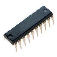
MCR908JK1ECPE Freescale Semiconductor, MCR908JK1ECPE Datasheet - Page 73

MCR908JK1ECPE
Manufacturer Part Number
MCR908JK1ECPE
Description
IC MCU 1.5K FLASH 8MHZ 20-DIP
Manufacturer
Freescale Semiconductor
Series
HC08r
Datasheet
1.MC908JK1ECDWE.pdf
(180 pages)
Specifications of MCR908JK1ECPE
Core Processor
HC08
Core Size
8-Bit
Speed
8MHz
Peripherals
LED, LVD, POR, PWM
Number Of I /o
14
Program Memory Size
1.5KB (1.5K x 8)
Program Memory Type
FLASH
Ram Size
128 x 8
Voltage - Supply (vcc/vdd)
2.7 V ~ 3.3 V
Data Converters
A/D 12x8b
Oscillator Type
External
Operating Temperature
-40°C ~ 85°C
Package / Case
20-DIP (0.300", 7.62mm)
Processor Series
HC08JK
Core
HC08
Data Bus Width
8 bit
Data Ram Size
128 B
Maximum Clock Frequency
8 MHz
Number Of Programmable I/os
15
Number Of Timers
2
Maximum Operating Temperature
+ 85 C
Mounting Style
Through Hole
Development Tools By Supplier
FSICEBASE, DEMO908JL16E, M68CBL05CE
Minimum Operating Temperature
- 40 C
On-chip Adc
8 bit, 12 Channel
Lead Free Status / RoHS Status
Lead free / RoHS Compliant
Eeprom Size
-
Connectivity
-
Lead Free Status / Rohs Status
Details
Available stocks
Company
Part Number
Manufacturer
Quantity
Price
Company:
Part Number:
MCR908JK1ECPE
Manufacturer:
Freescale Semiconductor
Quantity:
135
7.3.1 Entering Monitor Mode
Table 7-1
may be entered after a POR and will allow communication at 9600 baud provided one of the following sets
of conditions is met:
If V
frequency is a divide-by-two of the clock input to OSC1. If PTB3 is high with V
monitor mode entry
OSC1. Holding the PTB3 pin low when entering monitor mode causes a bypass of a divide-by-two stage
at the oscillator only if V
2OSCOUT frequency, and OSC1 input directly generates internal bus clocks. In this case, the OSC1
signal must have a 50% duty cycle at maximum bus frequency.
Freescale Semiconductor
1. PTB3 = 0: Bypasses the divide-by-two prescaler to SIM when using V
2. See
3. For IRQ = V
4. For IRQ = V
1. If IRQ = V
2. If IRQ = V
3. If $FFFE & $FFFF is blank (contains $FF):
TST
V
The OSC1 clock must be 50% duty cycle for this condition.
V
TST
V
V
IRQ
MC68HRC908JL3E/JK3E/JK1E — clock must be EXT OSC.
MC68HC908JL3E/JK3E/JK1E — clock can be EXT OSC or XTAL.
MC68HRC908JL3E/JK3E/JK1E — clock must be RC OSC.
MC68HC908JL3E/JK3E/JK1E — clock can be EXT OSC or XTAL.
TST
DD
DD
–
–
–
–
–
–
Table 16-4. DC Electrical Characteristics (5V)
is applied to IRQ and PTB3 is low upon monitor mode entry
(2)
shows the pin conditions for entering monitor mode. As specified in the table, monitor mode
Clock on OSC1 is 4.9125MHz (EXT OSC or XTAL)
PTB3 = low
Clock on OSC1 is 9.8304MHz (EXT OSC or XTAL)
PTB3 = high
Clock on OSC1 is 9.8304MHz (EXT OSC or XTAL or RC)
IRQ = V
TST
DD
(contain
:
BLANK
BLANK
:
TST
TST
$FF)
NOT
X
X
DD
(Table 7-1
:
:
Table 7-1. Monitor Mode Entry Requirements and Options
TST
X
X
0
1
is applied to IRQ. In this event, the OSCOUT frequency is equal to the
0
0
X
X
condition set 2), the bus frequency is a divide-by-four of the clock input to
MC68HC908JL3E Family Data Sheet, Rev. 4
X
X
1
1
1
1
1
X
OSC1 Frequency
for V
4.9152MHz
9.8304MHz
9.8304MHz
At desired
frequency
TST
voltage level requirements.
TST
for monitor mode entry.
2.4576MHz
2.4576MHz
2.4576MHz
Frequency
(OSC1 ÷ 2)
(OSC1 ÷ 4)
(OSC1 ÷ 4)
OSC1 ÷ 4
Bus
(Table 7-1
TST
High-voltage entry to monitor
mode.
9600 baud communication on
PTB0. COP disabled.
Low-voltage entry to monitor
mode.
9600 baud communication on
PTB0. COP disabled.
Enters User mode.
condition set 1), the bus
applied to IRQ upon
Functional Description
(3)
(4)
Comments
73


