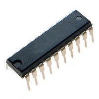
MCR908JK1ECPE Freescale Semiconductor, MCR908JK1ECPE Datasheet - Page 31

MCR908JK1ECPE
Manufacturer Part Number
MCR908JK1ECPE
Description
IC MCU 1.5K FLASH 8MHZ 20-DIP
Manufacturer
Freescale Semiconductor
Series
HC08r
Datasheet
1.MC908JK1ECDWE.pdf
(180 pages)
Specifications of MCR908JK1ECPE
Core Processor
HC08
Core Size
8-Bit
Speed
8MHz
Peripherals
LED, LVD, POR, PWM
Number Of I /o
14
Program Memory Size
1.5KB (1.5K x 8)
Program Memory Type
FLASH
Ram Size
128 x 8
Voltage - Supply (vcc/vdd)
2.7 V ~ 3.3 V
Data Converters
A/D 12x8b
Oscillator Type
External
Operating Temperature
-40°C ~ 85°C
Package / Case
20-DIP (0.300", 7.62mm)
Processor Series
HC08JK
Core
HC08
Data Bus Width
8 bit
Data Ram Size
128 B
Maximum Clock Frequency
8 MHz
Number Of Programmable I/os
15
Number Of Timers
2
Maximum Operating Temperature
+ 85 C
Mounting Style
Through Hole
Development Tools By Supplier
FSICEBASE, DEMO908JL16E, M68CBL05CE
Minimum Operating Temperature
- 40 C
On-chip Adc
8 bit, 12 Channel
Lead Free Status / RoHS Status
Lead free / RoHS Compliant
Eeprom Size
-
Connectivity
-
Lead Free Status / Rohs Status
Details
Available stocks
Company
Part Number
Manufacturer
Quantity
Price
Company:
Part Number:
MCR908JK1ECPE
Manufacturer:
Freescale Semiconductor
Quantity:
135
2.10 Flash Program Operation
Programming of the Flash memory is done on a row basis. A row consists of 32 consecutive bytes starting
from addresses $XX00, $XX20, $XX40, $XX60, $XX80, $XXA0, $XXC0 or $XXE0. Use this step-by-step
procedure to program a row of Flash memory
algorithm):
This program sequence is repeated throughout the memory until all data is programmed.
2.11 Flash Protection
Due to the ability of the on-board charge pump to erase and program the Flash memory in the target
application, provision is made to protect blocks of memory from unintentional erase or program operations
due to system malfunction. This protection is done by use of a Flash Block Protect Register (FLBPR). The
FLBPR determines the range of the Flash memory which is to be protected. The range of the protected
area starts from a location defined by FLBPR and ends to the bottom of the Flash memory ($FFFF). When
the memory is protected, the HVEN bit cannot be set in either ERASE or PROGRAM operations.
Freescale Semiconductor
10. Wait for time, t
11. Clear the HVEN bit.
12. After time, t
1. Set the PGM bit. This configures the memory for program operation and enables the latching of
2. Write any data to any Flash location within the address range of the row to be programmed.
3. Wait for a time, t
4. Set the HVEN bit.
5. Wait for a time, t
6. Write data to the byte being programmed.
7. Wait for time, t
8. Repeat step 6 and 7 until all the bytes within the row are programmed.
9. Clear the PGM bit.
address and data for programming.
The time between each Flash address change (step 6 to step 6), or the time
between the last Flash addressed programmed to clearing the PGM bit
(step 6 to step 10), must not exceed the maximum programming time,
t
Programming and erasing of Flash locations cannot be performed by code
being executed from the Flash memory. While these operations must be
performed in the order shown, other unrelated operations may occur
between the steps.
PROG
rcv
PROG
nvh
(1μs), the memory can be accessed in read mode again.
max.
nvs
pgs
(5μs).
(10μs).
(5μs).
(30μs).
MC68HC908JL3E Family Data Sheet, Rev. 4
(Figure 2-5
NOTE
NOTE
shows a flowchart of the programming
Flash Program Operation
31


