MC9S08DZ60MLC Freescale Semiconductor, MC9S08DZ60MLC Datasheet - Page 12
MC9S08DZ60MLC
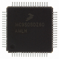
Manufacturer Part Number
MC9S08DZ60MLC
Description
IC MCU 60K FLASH 4K RAM 32-LQFP
Manufacturer
Freescale Semiconductor
Series
HCS08r
Specifications of MC9S08DZ60MLC
Core Processor
HCS08
Core Size
8-Bit
Speed
40MHz
Connectivity
CAN, I²C, LIN, SCI, SPI
Peripherals
LVD, POR, PWM, WDT
Number Of I /o
25
Program Memory Size
60KB (60K x 8)
Program Memory Type
FLASH
Eeprom Size
2K x 8
Ram Size
4K x 8
Voltage - Supply (vcc/vdd)
2.7 V ~ 5.5 V
Data Converters
A/D 10x12b
Oscillator Type
External
Operating Temperature
-40°C ~ 125°C
Package / Case
32-LQFP
For Use With
DEMO9S08DZ60 - BOARD DEMOEVB9S08DZ60 - BOARD EVAL FOR 9S08DZ60
Lead Free Status / RoHS Status
Lead free / RoHS Compliant
Available stocks
Company
Part Number
Manufacturer
Quantity
Price
Company:

Part Number:
MC9S08DZ60MLC
Manufacturer:
Freescale Semiconductor
Quantity:
10 000


Section Number
8.2
8.3
8.4
8.5
9.1
9.2
9.3
9.4
10.1 Introduction ....................................................................................................................................173
12
External Signal Description ...........................................................................................................139
Register Definition .........................................................................................................................140
Functional Description ...................................................................................................................146
Initialization / Application Information .........................................................................................152
Introduction ....................................................................................................................................167
External Signal Description ...........................................................................................................170
Memory Map/Register Definition ..................................................................................................171
Functional Description ...................................................................................................................172
8.1.2 Modes of Operation ........................................................................................................139
8.3.1 MCG Control Register 1 (MCGC1) ...............................................................................140
8.3.2 MCG Control Register 2 (MCGC2) ...............................................................................141
8.3.3 MCG Trim Register (MCGTRM) ...................................................................................142
8.3.4 MCG Status and Control Register (MCGSC) .................................................................143
8.3.5 MCG Control Register 3 (MCGC3) ...............................................................................144
8.4.1 Operational Modes ..........................................................................................................146
8.4.2 Mode Switching ..............................................................................................................150
8.4.3 Bus Frequency Divider ...................................................................................................151
8.4.4 Low Power Bit Usage .....................................................................................................151
8.4.5 Internal Reference Clock ................................................................................................151
8.4.6 External Reference Clock ...............................................................................................151
8.4.7 Fixed Frequency Clock ...................................................................................................152
8.5.1 MCG Module Initialization Sequence ............................................................................152
8.5.2 MCG Mode Switching ....................................................................................................153
8.5.3 Calibrating the Internal Reference Clock (IRC) .............................................................164
9.1.1 ACMP Configuration Information ..................................................................................167
9.1.2 Features ...........................................................................................................................169
9.1.3 Modes of Operation ........................................................................................................169
9.1.4 Block Diagram ................................................................................................................170
9.3.1 ACMPx Status and Control Register (ACMPxSC) .........................................................171
10.1.1 Analog Power and Ground Signal Names ......................................................................173
10.1.2 Channel Assignments ......................................................................................................173
10.1.3 Alternate Clock ...............................................................................................................174
10.1.4 Hardware Trigger ............................................................................................................174
10.1.5 Temperature Sensor ........................................................................................................175
10.1.6 Features ...........................................................................................................................177
Analog-to-Digital Converter (S08ADC12V1)
Analog Comparator (S08ACMPV3)
MC9S08DZ60 Series Data Sheet, Rev. 4
Chapter 10
Chapter 9
Title
Freescale Semiconductor
Page
Related parts for MC9S08DZ60MLC
Image
Part Number
Description
Manufacturer
Datasheet
Request
R

Part Number:
Description:
Manufacturer:
Freescale Semiconductor, Inc
Datasheet:
Part Number:
Description:
Manufacturer:
Freescale Semiconductor, Inc
Datasheet:
Part Number:
Description:
Manufacturer:
Freescale Semiconductor, Inc
Datasheet:
Part Number:
Description:
Manufacturer:
Freescale Semiconductor, Inc
Datasheet:
Part Number:
Description:
Manufacturer:
Freescale Semiconductor, Inc
Datasheet:
Part Number:
Description:
Manufacturer:
Freescale Semiconductor, Inc
Datasheet:
Part Number:
Description:
Manufacturer:
Freescale Semiconductor, Inc
Datasheet:
Part Number:
Description:
Manufacturer:
Freescale Semiconductor, Inc
Datasheet:
Part Number:
Description:
Manufacturer:
Freescale Semiconductor, Inc
Datasheet:
Part Number:
Description:
Manufacturer:
Freescale Semiconductor, Inc
Datasheet:
Part Number:
Description:
Manufacturer:
Freescale Semiconductor, Inc
Datasheet:
Part Number:
Description:
Manufacturer:
Freescale Semiconductor, Inc
Datasheet:
Part Number:
Description:
Manufacturer:
Freescale Semiconductor, Inc
Datasheet:
Part Number:
Description:
Manufacturer:
Freescale Semiconductor, Inc
Datasheet:
Part Number:
Description:
Manufacturer:
Freescale Semiconductor, Inc
Datasheet: