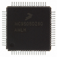
MC9S08DZ60MLC Freescale Semiconductor, MC9S08DZ60MLC Datasheet - Page 401

MC9S08DZ60MLC
Manufacturer Part Number
MC9S08DZ60MLC
Description
IC MCU 60K FLASH 4K RAM 32-LQFP
Manufacturer
Freescale Semiconductor
Series
HCS08r
Specifications of MC9S08DZ60MLC
Core Processor
HCS08
Core Size
8-Bit
Speed
40MHz
Connectivity
CAN, I²C, LIN, SCI, SPI
Peripherals
LVD, POR, PWM, WDT
Number Of I /o
25
Program Memory Size
60KB (60K x 8)
Program Memory Type
FLASH
Eeprom Size
2K x 8
Ram Size
4K x 8
Voltage - Supply (vcc/vdd)
2.7 V ~ 5.5 V
Data Converters
A/D 10x12b
Oscillator Type
External
Operating Temperature
-40°C ~ 125°C
Package / Case
32-LQFP
For Use With
DEMO9S08DZ60 - BOARD DEMOEVB9S08DZ60 - BOARD EVAL FOR 9S08DZ60
Lead Free Status / RoHS Status
Lead free / RoHS Compliant
Available stocks
Company
Part Number
Manufacturer
Quantity
Price
Company:
Part Number:
MC9S08DZ60MLC
Manufacturer:
Freescale Semiconductor
Quantity:
10 000
- Current page: 401 of 416
- Download datasheet (5Mb)
An input capture event sets a flag bit (CHnF) that can optionally generate a CPU interrupt request.
B.3.2.2
With the output compare function, the TPM can generate timed pulses with programmable position,
polarity, duration, and frequency. When the counter reaches the value in the channel value registers of an
output compare channel, the TPM can set, clear, or toggle the channel pin.
In output compare mode, values are transferred to the corresponding timer channel value registers only
after both 8-bit bytes of a 16-bit register have been written. This coherency sequence can be manually reset
by writing to the channel status/control register (TPMxCnSC).
An output compare event sets a flag bit (CHnF) that can optionally generate a CPU interrupt request.
B.3.2.3
This type of PWM output uses the normal up-counting mode of the timer counter (CPWMS = 0) and can
be used when other channels in the same TPM are configured for input capture or output compare
functions. The period of this PWM signal is determined by the setting in the modulus register
(TPMxMODH:TPMxMODL). The duty cycle is determined by the setting in the timer channel value
register (TPMxCnVH:TPMxCnVL). The polarity of this PWM signal is determined by the setting in the
ELSnA control bit. Duty cycle cases of 0 percent and 100 percent are possible.
As
(duty cycle) of the PWM signal. The time between the modulus overflow and the output compare is the
pulse width. If ELSnA = 0, the counter overflow forces the PWM signal high and the output compare
forces the PWM signal low. If ELSnA = 1, the counter overflow forces the PWM signal low and the output
compare forces the PWM signal high.
When the channel value register is set to 0x0000, the duty cycle is 0 percent. By setting the timer channel
value register (TPMxCnVH:TPMxCnVL) to a value greater than the modulus setting, 100% duty cycle
can be achieved. This implies that the modulus setting must be less than 0xFFFF to get 100% duty cycle.
Because the HCS08 is a family of 8-bit MCUs, the settings in the timer channel registers are buffered to
ensure coherent 16-bit updates and to avoid unexpected PWM pulse widths. Writes to either register,
TPMxCnVH or TPMxCnVL, write to buffer registers. In edge-PWM mode, values are transferred to the
corresponding timer channel registers only after both 8-bit bytes of a 16-bit register have been written and
Freescale Semiconductor
Figure B-10
Output Compare Mode
Edge-Aligned PWM Mode
TPMxC
shows, the output compare value in the TPM channel registers determines the pulse width
OVERFLOW
Figure B-10. PWM Period and Pulse Width (ELSnA = 0)
PULSE
WIDTH
PERIOD
MC9S08DZ60 Series Data Sheet, Rev. 4
COMPARE
OUTPUT
OVERFLOW
COMPARE
OUTPUT
Appendix B Timer Pulse-Width Modulator (TPMV2)
OVERFLOW
COMPARE
OUTPUT
401
Related parts for MC9S08DZ60MLC
Image
Part Number
Description
Manufacturer
Datasheet
Request
R
Part Number:
Description:
Manufacturer:
Freescale Semiconductor, Inc
Datasheet:
Part Number:
Description:
Manufacturer:
Freescale Semiconductor, Inc
Datasheet:
Part Number:
Description:
Manufacturer:
Freescale Semiconductor, Inc
Datasheet:
Part Number:
Description:
Manufacturer:
Freescale Semiconductor, Inc
Datasheet:
Part Number:
Description:
Manufacturer:
Freescale Semiconductor, Inc
Datasheet:
Part Number:
Description:
Manufacturer:
Freescale Semiconductor, Inc
Datasheet:
Part Number:
Description:
Manufacturer:
Freescale Semiconductor, Inc
Datasheet:
Part Number:
Description:
Manufacturer:
Freescale Semiconductor, Inc
Datasheet:
Part Number:
Description:
Manufacturer:
Freescale Semiconductor, Inc
Datasheet:
Part Number:
Description:
Manufacturer:
Freescale Semiconductor, Inc
Datasheet:
Part Number:
Description:
Manufacturer:
Freescale Semiconductor, Inc
Datasheet:
Part Number:
Description:
Manufacturer:
Freescale Semiconductor, Inc
Datasheet:
Part Number:
Description:
Manufacturer:
Freescale Semiconductor, Inc
Datasheet:
Part Number:
Description:
Manufacturer:
Freescale Semiconductor, Inc
Datasheet:
Part Number:
Description:
Manufacturer:
Freescale Semiconductor, Inc
Datasheet:


