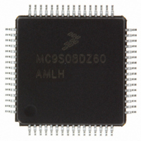
MC9S08DZ60MLC Freescale Semiconductor, MC9S08DZ60MLC Datasheet - Page 75

MC9S08DZ60MLC
Manufacturer Part Number
MC9S08DZ60MLC
Description
IC MCU 60K FLASH 4K RAM 32-LQFP
Manufacturer
Freescale Semiconductor
Series
HCS08r
Specifications of MC9S08DZ60MLC
Core Processor
HCS08
Core Size
8-Bit
Speed
40MHz
Connectivity
CAN, I²C, LIN, SCI, SPI
Peripherals
LVD, POR, PWM, WDT
Number Of I /o
25
Program Memory Size
60KB (60K x 8)
Program Memory Type
FLASH
Eeprom Size
2K x 8
Ram Size
4K x 8
Voltage - Supply (vcc/vdd)
2.7 V ~ 5.5 V
Data Converters
A/D 10x12b
Oscillator Type
External
Operating Temperature
-40°C ~ 125°C
Package / Case
32-LQFP
For Use With
DEMO9S08DZ60 - BOARD DEMOEVB9S08DZ60 - BOARD EVAL FOR 9S08DZ60
Lead Free Status / RoHS Status
Lead free / RoHS Compliant
Available stocks
Company
Part Number
Manufacturer
Quantity
Price
Company:
Part Number:
MC9S08DZ60MLC
Manufacturer:
Freescale Semiconductor
Quantity:
10 000
- Current page: 75 of 416
- Download datasheet (5Mb)
5.6
The MC9S08DZ60 Series includes a system to protect against low-voltage conditions in order to protect
memory contents and control MCU system states during supply voltage variations. The system is
comprised of a power-on reset (POR) circuit and a LVD circuit with trip voltages for warning and
detection. The LVD circuit is enabled when LVDE in SPMSC1 is set to 1. The LVD is disabled upon
entering any of the stop modes unless LVDSE is set in SPMSC1. If LVDSE and LVDE are both set, then
the MCU cannot enter stop2 (it will enter stop3 instead), and the current consumption in stop3 with the
LVD enabled will be higher.
5.6.1
When power is initially applied to the MCU, or when the supply voltage drops below the power-on reset
rearm voltage level, V
LVD circuit will hold the MCU in reset until the supply has risen above the low-voltage detection low
threshold, V
5.6.2
The LVD can be configured to generate a reset upon detection of a low-voltage condition by setting
LVDRE to 1. The low-voltage detection threshold is determined by the LVDV bit. After an LVD reset has
occurred, the LVD system will hold the MCU in reset until the supply voltage has risen above the
low-voltage detection threshold. The LVD bit in the SRS register is set following either an LVD reset or
POR.
5.6.3
The LVD system has a low-voltage warning flag to indicate to the user that the supply voltage is
approaching the low-voltage condition. When a low-voltage warning condition is detected and is
configured for interrupt operation (LVWIE set to 1), LVWF in SPMSC1 will be set and an LVW interrupt
request will occur.
5.7
The PTA0 pin is shared with the MCLK clock output. If the MCSEL bits are all zeroes, the MCLK clock
is disabled. Setting any of the MCSEL bits causes the PTA0 pin to output a divided version of the internal
MCU bus clock regardless of the state of the port data direction control bit for the pin. The divide ratio is
determined by the MCSEL bits. The slew rate and drive strength for the pin are controlled by PTASE0 and
PTADS0, respectively. The maximum clock output frequency is limited if slew rate control is enabled, see
the electrical specifications for the maximum frequency under different conditions.
Freescale Semiconductor
Low-Voltage Detect (LVD) System
MCLK Output
Power-On Reset Operation
Low-Voltage Detection (LVD) Reset Operation
Low-Voltage Warning (LVW) Interrupt Operation
LVDL
. Both the POR bit and the LVD bit in SRS are set following a POR.
POR
, the POR circuit will cause a reset condition. As the supply voltage rises, the
MC9S08DZ60 Series Data Sheet, Rev. 4
Chapter 5 Resets, Interrupts, and General System Control
75
Related parts for MC9S08DZ60MLC
Image
Part Number
Description
Manufacturer
Datasheet
Request
R
Part Number:
Description:
Manufacturer:
Freescale Semiconductor, Inc
Datasheet:
Part Number:
Description:
Manufacturer:
Freescale Semiconductor, Inc
Datasheet:
Part Number:
Description:
Manufacturer:
Freescale Semiconductor, Inc
Datasheet:
Part Number:
Description:
Manufacturer:
Freescale Semiconductor, Inc
Datasheet:
Part Number:
Description:
Manufacturer:
Freescale Semiconductor, Inc
Datasheet:
Part Number:
Description:
Manufacturer:
Freescale Semiconductor, Inc
Datasheet:
Part Number:
Description:
Manufacturer:
Freescale Semiconductor, Inc
Datasheet:
Part Number:
Description:
Manufacturer:
Freescale Semiconductor, Inc
Datasheet:
Part Number:
Description:
Manufacturer:
Freescale Semiconductor, Inc
Datasheet:
Part Number:
Description:
Manufacturer:
Freescale Semiconductor, Inc
Datasheet:
Part Number:
Description:
Manufacturer:
Freescale Semiconductor, Inc
Datasheet:
Part Number:
Description:
Manufacturer:
Freescale Semiconductor, Inc
Datasheet:
Part Number:
Description:
Manufacturer:
Freescale Semiconductor, Inc
Datasheet:
Part Number:
Description:
Manufacturer:
Freescale Semiconductor, Inc
Datasheet:
Part Number:
Description:
Manufacturer:
Freescale Semiconductor, Inc
Datasheet:


