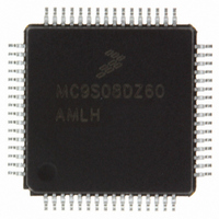
MC9S08DZ60MLC Freescale Semiconductor, MC9S08DZ60MLC Datasheet - Page 161

MC9S08DZ60MLC
Manufacturer Part Number
MC9S08DZ60MLC
Description
IC MCU 60K FLASH 4K RAM 32-LQFP
Manufacturer
Freescale Semiconductor
Series
HCS08r
Specifications of MC9S08DZ60MLC
Core Processor
HCS08
Core Size
8-Bit
Speed
40MHz
Connectivity
CAN, I²C, LIN, SCI, SPI
Peripherals
LVD, POR, PWM, WDT
Number Of I /o
25
Program Memory Size
60KB (60K x 8)
Program Memory Type
FLASH
Eeprom Size
2K x 8
Ram Size
4K x 8
Voltage - Supply (vcc/vdd)
2.7 V ~ 5.5 V
Data Converters
A/D 10x12b
Oscillator Type
External
Operating Temperature
-40°C ~ 125°C
Package / Case
32-LQFP
For Use With
DEMO9S08DZ60 - BOARD DEMOEVB9S08DZ60 - BOARD EVAL FOR 9S08DZ60
Lead Free Status / RoHS Status
Lead free / RoHS Compliant
Available stocks
Company
Part Number
Manufacturer
Quantity
Price
Company:
Part Number:
MC9S08DZ60MLC
Manufacturer:
Freescale Semiconductor
Quantity:
10 000
- Current page: 161 of 416
- Download datasheet (5Mb)
external crystal and a maximum reference divider factor of 128, the resulting frequency of the reference
clock for the FLL is 62.5 kHz (greater than the 39.0625 kHz maximum allowed).
Care must be taken in the software to minimize the amount of time spent in this state where the FLL is
operating in this condition.
The following code sequence describes how to move from FEI mode to PEE mode until the 8 MHz crystal
reference frequency is set to achieve a bus frequency of 8 MHz. Because the MCG is in FEI mode out of
reset, this example also shows how to initialize the MCG for PEE mode out of reset. First, the code
sequence will be described. Then a flowchart will be included which illustrates the sequence.
Freescale Semiconductor
1. First, FEI must transition to FBE mode:
2. Then, FBE mode transitions into BLPE mode:
a) MCGC2 = 0x36 (%00110110)
b) Loop until OSCINIT (bit 1) in MCGSC is 1, indicating the crystal selected by the EREFS bit
c) Block Interrupts (If applicable by setting the interrupt bit in the CCR).
d) MCGC1 = 0xB8 (%10111000)
e) Loop until IREFST (bit 4) in MCGSC is 0, indicating the external reference is the current
f) Loop until CLKST (bits 3 and 2) in MCGSC are %10, indicating that the external reference
a) MCGC2 = 0x3E (%00111110)
b) Enable Interrupts (if applicable by clearing the interrupt bit in the CCR).
– BDIV (bits 7 and 6) set to %00, or divide-by-1
– RANGE (bit 5) set to 1 because the frequency of 8 MHz is within the high frequency range
– HGO (bit 4) set to 1 to configure external oscillator for high gain operation
– EREFS (bit 2) set to 1, because a crystal is being used
– ERCLKEN (bit 1) set to 1 to ensure the external reference clock is active
has been initialized.
– CLKS (bits 7 and 6) set to %10 in order to select external reference clock as system clock
– RDIV (bits 5-3) set to %111, or divide-by-128.
– IREFS (bit 2) cleared to 0, selecting the external reference clock
source for the reference clock
clock is selected to feed MCGOUT
– LP (bit 3) in MCGC2 to 1 (BLPE mode entered)
source
8 MHz / 128 = 62.5 kHz which is greater than the 31.25 kHz to 39.0625 kHz
range required by the FLL. Therefore after the transition to FBE is
complete, software must progress through to BLPE mode immediately by
setting the LP bit in MCGC2.
There must be no extra steps (including interrupts) between steps 1d and 2a.
MC9S08DZ60 Series Data Sheet, Rev. 4
NOTE
NOTE
Chapter 8 Multi-Purpose Clock Generator (S08MCGV1)
161
Related parts for MC9S08DZ60MLC
Image
Part Number
Description
Manufacturer
Datasheet
Request
R
Part Number:
Description:
Manufacturer:
Freescale Semiconductor, Inc
Datasheet:
Part Number:
Description:
Manufacturer:
Freescale Semiconductor, Inc
Datasheet:
Part Number:
Description:
Manufacturer:
Freescale Semiconductor, Inc
Datasheet:
Part Number:
Description:
Manufacturer:
Freescale Semiconductor, Inc
Datasheet:
Part Number:
Description:
Manufacturer:
Freescale Semiconductor, Inc
Datasheet:
Part Number:
Description:
Manufacturer:
Freescale Semiconductor, Inc
Datasheet:
Part Number:
Description:
Manufacturer:
Freescale Semiconductor, Inc
Datasheet:
Part Number:
Description:
Manufacturer:
Freescale Semiconductor, Inc
Datasheet:
Part Number:
Description:
Manufacturer:
Freescale Semiconductor, Inc
Datasheet:
Part Number:
Description:
Manufacturer:
Freescale Semiconductor, Inc
Datasheet:
Part Number:
Description:
Manufacturer:
Freescale Semiconductor, Inc
Datasheet:
Part Number:
Description:
Manufacturer:
Freescale Semiconductor, Inc
Datasheet:
Part Number:
Description:
Manufacturer:
Freescale Semiconductor, Inc
Datasheet:
Part Number:
Description:
Manufacturer:
Freescale Semiconductor, Inc
Datasheet:
Part Number:
Description:
Manufacturer:
Freescale Semiconductor, Inc
Datasheet:


