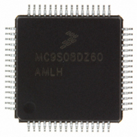
MC9S08DZ60MLC Freescale Semiconductor, MC9S08DZ60MLC Datasheet - Page 295

MC9S08DZ60MLC
Manufacturer Part Number
MC9S08DZ60MLC
Description
IC MCU 60K FLASH 4K RAM 32-LQFP
Manufacturer
Freescale Semiconductor
Series
HCS08r
Specifications of MC9S08DZ60MLC
Core Processor
HCS08
Core Size
8-Bit
Speed
40MHz
Connectivity
CAN, I²C, LIN, SCI, SPI
Peripherals
LVD, POR, PWM, WDT
Number Of I /o
25
Program Memory Size
60KB (60K x 8)
Program Memory Type
FLASH
Eeprom Size
2K x 8
Ram Size
4K x 8
Voltage - Supply (vcc/vdd)
2.7 V ~ 5.5 V
Data Converters
A/D 10x12b
Oscillator Type
External
Operating Temperature
-40°C ~ 125°C
Package / Case
32-LQFP
For Use With
DEMO9S08DZ60 - BOARD DEMOEVB9S08DZ60 - BOARD EVAL FOR 9S08DZ60
Lead Free Status / RoHS Status
Lead free / RoHS Compliant
Available stocks
Company
Part Number
Manufacturer
Quantity
Price
Company:
Part Number:
MC9S08DZ60MLC
Manufacturer:
Freescale Semiconductor
Quantity:
10 000
- Current page: 295 of 416
- Download datasheet (5Mb)
14.2.2
This read/write register is used to control various optional features of the SCI system.
Freescale Semiconductor
SCISWAI
SBR[7:0]
Reset
Reset
LOOPS
RSRC
Field
Field
7:0
M
7
6
5
4
W
W
R
R
LOOPS
SBR7
SCI Control Register 1 (SCIxC1)
Baud Rate Modulo Divisor — These 13 bits in SBR[12:0] are referred to collectively as BR, and they set the
modulo divide rate for the SCI baud rate generator. When BR = 0, the SCI baud rate generator is disabled to
reduce supply current. When BR = 1 to 8191, the SCI baud rate = BUSCLK/(16×BR). See also BR bits in
Table
Loop Mode Select — Selects between loop back modes and normal 2-pin full-duplex modes. When
LOOPS = 1, the transmitter output is internally connected to the receiver input.
0 Normal operation — RxD and TxD use separate pins.
1 Loop mode or single-wire mode where transmitter outputs are internally connected to receiver input. (See
SCI Stops in Wait Mode
0 SCI clocks continue to run in wait mode so the SCI can be the source of an interrupt that wakes up the CPU.
1 SCI clocks freeze while CPU is in wait mode.
Receiver Source Select — This bit has no meaning or effect unless the LOOPS bit is set to 1. When
LOOPS = 1, the receiver input is internally connected to the TxD pin and RSRC determines whether this
connection is also connected to the transmitter output.
0 Provided LOOPS = 1, RSRC = 0 selects internal loop back mode and the SCI does not use the RxD pins.
1 Single-wire SCI mode where the TxD pin is connected to the transmitter output and receiver input.
9-Bit or 8-Bit Mode Select
0 Normal — start + 8 data bits (LSB first) + stop.
1 Receiver and transmitter use 9-bit data characters
0
0
7
7
RSRC
start + 8 data bits (LSB first) + 9th data bit + stop.
14-2.
bit.) RxD pin is not used by SCI.
SCISWAI
SBR6
0
0
6
6
Figure 14-5. SCI Baud Rate Register (SCIxBDL)
Figure 14-6. SCI Control Register 1 (SCIxC1)
Table 14-3. SCIxBDL Field Descriptions
Table 14-4. SCIxC1 Field Descriptions
MC9S08DZ60 Series Data Sheet, Rev. 4
RSRC
SBR5
0
0
5
5
SBR4
M
0
0
4
4
Description
Description
WAKE
SBR3
Chapter 14 Serial Communications Interface (S08SCIV4)
3
0
3
0
SBR2
ILT
1
0
2
2
SBR1
PE
0
0
1
1
SBR0
PT
0
0
0
0
295
Related parts for MC9S08DZ60MLC
Image
Part Number
Description
Manufacturer
Datasheet
Request
R
Part Number:
Description:
Manufacturer:
Freescale Semiconductor, Inc
Datasheet:
Part Number:
Description:
Manufacturer:
Freescale Semiconductor, Inc
Datasheet:
Part Number:
Description:
Manufacturer:
Freescale Semiconductor, Inc
Datasheet:
Part Number:
Description:
Manufacturer:
Freescale Semiconductor, Inc
Datasheet:
Part Number:
Description:
Manufacturer:
Freescale Semiconductor, Inc
Datasheet:
Part Number:
Description:
Manufacturer:
Freescale Semiconductor, Inc
Datasheet:
Part Number:
Description:
Manufacturer:
Freescale Semiconductor, Inc
Datasheet:
Part Number:
Description:
Manufacturer:
Freescale Semiconductor, Inc
Datasheet:
Part Number:
Description:
Manufacturer:
Freescale Semiconductor, Inc
Datasheet:
Part Number:
Description:
Manufacturer:
Freescale Semiconductor, Inc
Datasheet:
Part Number:
Description:
Manufacturer:
Freescale Semiconductor, Inc
Datasheet:
Part Number:
Description:
Manufacturer:
Freescale Semiconductor, Inc
Datasheet:
Part Number:
Description:
Manufacturer:
Freescale Semiconductor, Inc
Datasheet:
Part Number:
Description:
Manufacturer:
Freescale Semiconductor, Inc
Datasheet:
Part Number:
Description:
Manufacturer:
Freescale Semiconductor, Inc
Datasheet:


