MC9S08DZ60MLC Freescale Semiconductor, MC9S08DZ60MLC Datasheet - Page 37
MC9S08DZ60MLC
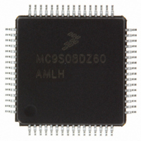
Manufacturer Part Number
MC9S08DZ60MLC
Description
IC MCU 60K FLASH 4K RAM 32-LQFP
Manufacturer
Freescale Semiconductor
Series
HCS08r
Specifications of MC9S08DZ60MLC
Core Processor
HCS08
Core Size
8-Bit
Speed
40MHz
Connectivity
CAN, I²C, LIN, SCI, SPI
Peripherals
LVD, POR, PWM, WDT
Number Of I /o
25
Program Memory Size
60KB (60K x 8)
Program Memory Type
FLASH
Eeprom Size
2K x 8
Ram Size
4K x 8
Voltage - Supply (vcc/vdd)
2.7 V ~ 5.5 V
Data Converters
A/D 10x12b
Oscillator Type
External
Operating Temperature
-40°C ~ 125°C
Package / Case
32-LQFP
For Use With
DEMO9S08DZ60 - BOARD DEMOEVB9S08DZ60 - BOARD EVAL FOR 9S08DZ60
Lead Free Status / RoHS Status
Lead free / RoHS Compliant
Available stocks
Company
Part Number
Manufacturer
Quantity
Price
Company:

Part Number:
MC9S08DZ60MLC
Manufacturer:
Freescale Semiconductor
Quantity:
10 000


1
2
3.6
One of two stop modes is entered upon execution of a STOP instruction when the STOPE bit in SOPT1
register is set. In both stop modes, all internal clocks are halted. The MCG module can be configured to
leave the reference clocks running. See
more information.
Table 3-1
conditions. The selected mode is entered following the execution of a STOP instruction.
3.6.1
Stop3 mode is entered by executing a STOP instruction under the conditions as shown in
states of all of the internal registers and logic, RAM contents, and I/O pin states are maintained.
Exit from stop3 is done by asserting RESET or an asynchronous interrupt pin. The asynchronous interrupt
pins are IRQ, PIA0–PIA7, PIB0–PIB7, and PID0–PID7. Exit from stop3 can also be done by the
low-voltage detect (LVD) reset, low-voltage warning (LVW) interrupt, ADC conversion complete
interrupt, real-time clock (RTC) interrupt, MSCAN wake-up interrupt, or SCI receiver interrupt.
If stop3 is exited by means of the RESET pin, the MCU will be reset and operation will resume after
fetching the reset vector. Exit by means of an interrupt will result in the MCU fetching the appropriate
interrupt vector.
3.6.1.1
The LVD system is capable of generating either an interrupt or a reset when the supply voltage drops below
the LVD voltage. If the LVD is enabled in stop (LVDE and LVDSE bits in SPMSC1 both set) at the time
the CPU executes a STOP instruction, then the voltage regulator remains active during stop mode.
For the ADC to operate the LVD must be left enabled when entering stop3.
Freescale Semiconductor
STOPE
ENBDM is located in the BDCSCR, which is only accessible through BDC commands, see
Control Register
When in Stop3 mode with BDM enabled, The S
0
1
1
1
1
Stop Modes
shows all of the control bits that affect stop mode selection and the mode selected under various
ENBDM
Stop3 Mode
LVD Enabled in Stop3 Mode
1
0
0
0
x
(BDCSCR)”.
1
Both bits must be 1
LVDE
Either bit a 0
Either bit a 0
x
x
LVDSE
MC9S08DZ60 Series Data Sheet, Rev. 4
Table 3-1. Stop Mode Selection
PPDC
Chapter 8, “Multi-Purpose Clock Generator
x
x
x
0
1
IDD
will be near R
Stop modes disabled; illegal opcode reset if STOP instruction executed
Stop3 with BDM enabled
Stop3 with voltage regulator active
Stop3
Stop2
IDD
levels because internal clocks are enabled.
2
Stop Mode
Section 17.4.1.1, “BDC Status and
Chapter 3 Modes of Operation
(S08MCGV1),” for
Table
3-1. The
37
Related parts for MC9S08DZ60MLC
Image
Part Number
Description
Manufacturer
Datasheet
Request
R

Part Number:
Description:
Manufacturer:
Freescale Semiconductor, Inc
Datasheet:
Part Number:
Description:
Manufacturer:
Freescale Semiconductor, Inc
Datasheet:
Part Number:
Description:
Manufacturer:
Freescale Semiconductor, Inc
Datasheet:
Part Number:
Description:
Manufacturer:
Freescale Semiconductor, Inc
Datasheet:
Part Number:
Description:
Manufacturer:
Freescale Semiconductor, Inc
Datasheet:
Part Number:
Description:
Manufacturer:
Freescale Semiconductor, Inc
Datasheet:
Part Number:
Description:
Manufacturer:
Freescale Semiconductor, Inc
Datasheet:
Part Number:
Description:
Manufacturer:
Freescale Semiconductor, Inc
Datasheet:
Part Number:
Description:
Manufacturer:
Freescale Semiconductor, Inc
Datasheet:
Part Number:
Description:
Manufacturer:
Freescale Semiconductor, Inc
Datasheet:
Part Number:
Description:
Manufacturer:
Freescale Semiconductor, Inc
Datasheet:
Part Number:
Description:
Manufacturer:
Freescale Semiconductor, Inc
Datasheet:
Part Number:
Description:
Manufacturer:
Freescale Semiconductor, Inc
Datasheet:
Part Number:
Description:
Manufacturer:
Freescale Semiconductor, Inc
Datasheet:
Part Number:
Description:
Manufacturer:
Freescale Semiconductor, Inc
Datasheet: