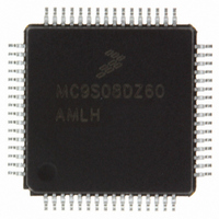
MC9S08DZ60MLC Freescale Semiconductor, MC9S08DZ60MLC Datasheet - Page 241

MC9S08DZ60MLC
Manufacturer Part Number
MC9S08DZ60MLC
Description
IC MCU 60K FLASH 4K RAM 32-LQFP
Manufacturer
Freescale Semiconductor
Series
HCS08r
Specifications of MC9S08DZ60MLC
Core Processor
HCS08
Core Size
8-Bit
Speed
40MHz
Connectivity
CAN, I²C, LIN, SCI, SPI
Peripherals
LVD, POR, PWM, WDT
Number Of I /o
25
Program Memory Size
60KB (60K x 8)
Program Memory Type
FLASH
Eeprom Size
2K x 8
Ram Size
4K x 8
Voltage - Supply (vcc/vdd)
2.7 V ~ 5.5 V
Data Converters
A/D 10x12b
Oscillator Type
External
Operating Temperature
-40°C ~ 125°C
Package / Case
32-LQFP
For Use With
DEMO9S08DZ60 - BOARD DEMOEVB9S08DZ60 - BOARD EVAL FOR 9S08DZ60
Lead Free Status / RoHS Status
Lead free / RoHS Compliant
Available stocks
Company
Part Number
Manufacturer
Quantity
Price
Company:
Part Number:
MC9S08DZ60MLC
Manufacturer:
Freescale Semiconductor
Quantity:
10 000
- Current page: 241 of 416
- Download datasheet (5Mb)
Read: Anytime
Write: Anytime in initialization mode (INITRQ = 1 and INITAK = 1)
12.4
The following section details the organization of the receive and transmit message buffers and the
associated control registers.
To simplify the programmer interface, the receive and transmit message buffers have the same outline.
Each message buffer allocates 16 bytes in the memory map containing a 13 byte data structure.
An additional transmit buffer priority register (TBPR) is defined for the transmit buffers. Within the last
two bytes of this memory map, the MSCAN stores a special 16-bit time stamp, which is sampled from an
internal timer after successful transmission or reception of a message. This feature is only available for
transmit and receiver buffers if the TIME bit is set (see
(CANCTL0)”).
The time stamp register is written by the MSCAN. The CPU can only read these registers.
Freescale Semiconductor
AM[7:0]
AM[7:0]
Field
Field
7:0
7:0
Reset
W
Figure 12-22. MSCAN Identifier Mask Registers (Second Bank) — CANIDMR4–CANIDMR7
R
Programmer’s Model of Message Storage
Acceptance Mask Bits — If a particular bit in this register is cleared, this indicates that the corresponding bit in
the identifier acceptance register must be the same as its identifier bit before a match is detected. The message
is accepted if all such bits match. If a bit is set, it indicates that the state of the corresponding bit in the identifier
acceptance register does not affect whether or not the message is accepted.
0 Match corresponding acceptance code register and identifier bits
1 Ignore corresponding acceptance code register bit (don’t care)
AM7
0
7
Table 12-22. CANIDMR0–CANIDMR3 Register Field Descriptions
Table 12-23. CANIDMR4–CANIDMR7 Register Field Descriptions
AM6
0
6
MC9S08DZ60 Series Data Sheet, Rev. 4
AM5
0
5
AM4
0
4
Description
Description
Chapter 12 Freescale’s Controller Area Network (S08MSCANV1)
Section 12.3.1, “MSCAN Control Register 0
AM3
0
3
AM2
0
2
AM1
1
0
AM0
0
0
241
Related parts for MC9S08DZ60MLC
Image
Part Number
Description
Manufacturer
Datasheet
Request
R
Part Number:
Description:
Manufacturer:
Freescale Semiconductor, Inc
Datasheet:
Part Number:
Description:
Manufacturer:
Freescale Semiconductor, Inc
Datasheet:
Part Number:
Description:
Manufacturer:
Freescale Semiconductor, Inc
Datasheet:
Part Number:
Description:
Manufacturer:
Freescale Semiconductor, Inc
Datasheet:
Part Number:
Description:
Manufacturer:
Freescale Semiconductor, Inc
Datasheet:
Part Number:
Description:
Manufacturer:
Freescale Semiconductor, Inc
Datasheet:
Part Number:
Description:
Manufacturer:
Freescale Semiconductor, Inc
Datasheet:
Part Number:
Description:
Manufacturer:
Freescale Semiconductor, Inc
Datasheet:
Part Number:
Description:
Manufacturer:
Freescale Semiconductor, Inc
Datasheet:
Part Number:
Description:
Manufacturer:
Freescale Semiconductor, Inc
Datasheet:
Part Number:
Description:
Manufacturer:
Freescale Semiconductor, Inc
Datasheet:
Part Number:
Description:
Manufacturer:
Freescale Semiconductor, Inc
Datasheet:
Part Number:
Description:
Manufacturer:
Freescale Semiconductor, Inc
Datasheet:
Part Number:
Description:
Manufacturer:
Freescale Semiconductor, Inc
Datasheet:
Part Number:
Description:
Manufacturer:
Freescale Semiconductor, Inc
Datasheet:


