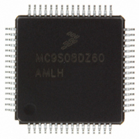
MC9S08DZ60MLC Freescale Semiconductor, MC9S08DZ60MLC Datasheet - Page 275

MC9S08DZ60MLC
Manufacturer Part Number
MC9S08DZ60MLC
Description
IC MCU 60K FLASH 4K RAM 32-LQFP
Manufacturer
Freescale Semiconductor
Series
HCS08r
Specifications of MC9S08DZ60MLC
Core Processor
HCS08
Core Size
8-Bit
Speed
40MHz
Connectivity
CAN, I²C, LIN, SCI, SPI
Peripherals
LVD, POR, PWM, WDT
Number Of I /o
25
Program Memory Size
60KB (60K x 8)
Program Memory Type
FLASH
Eeprom Size
2K x 8
Ram Size
4K x 8
Voltage - Supply (vcc/vdd)
2.7 V ~ 5.5 V
Data Converters
A/D 10x12b
Oscillator Type
External
Operating Temperature
-40°C ~ 125°C
Package / Case
32-LQFP
For Use With
DEMO9S08DZ60 - BOARD DEMOEVB9S08DZ60 - BOARD EVAL FOR 9S08DZ60
Lead Free Status / RoHS Status
Lead free / RoHS Compliant
Available stocks
Company
Part Number
Manufacturer
Quantity
Price
Company:
Part Number:
MC9S08DZ60MLC
Manufacturer:
Freescale Semiconductor
Quantity:
10 000
- Current page: 275 of 416
- Download datasheet (5Mb)
13.1.1
Features of the SPI module include:
13.1.2
This section includes block diagrams showing SPI system connections, the internal organization of the SPI
module, and the SPI clock dividers that control the master mode bit rate.
13.1.2.1
Figure 13-2
device initiates all SPI data transfers. During a transfer, the master shifts data out (on the MOSI pin) to the
slave while simultaneously shifting data in (on the MISO pin) from the slave. The transfer effectively
exchanges the data that was in the SPI shift registers of the two SPI systems. The SPSCK signal is a clock
output from the master and an input to the slave. The slave device must be selected by a low level on the
slave select input (SS pin). In this system, the master device has configured its SS pin as an optional slave
select output.
Freescale Semiconductor
•
•
•
•
•
•
•
Master or slave mode operation
Full-duplex or single-wire bidirectional option
Programmable transmit bit rate
Double-buffered transmit and receive
Serial clock phase and polarity options
Slave select output
Selectable MSB-first or LSB-first shifting
7
6
Features
Block Diagrams
shows the SPI modules of two MCUs connected in a master-slave arrangement. The master
SPI System Block Diagram
5
GENERATOR
SPI SHIFTER
MASTER
CLOCK
4
3
2
1
0
Figure 13-2. SPI System Connections
MC9S08DZ60 Series Data Sheet, Rev. 4
MOSI
MISO
SPSCK
SS
SPSCK
MOSI
MISO
SS
Chapter 13 Serial Peripheral Interface (S08SPIV3)
7
SLAVE
6
5
SPI SHIFTER
4
3
2
1
0
275
Related parts for MC9S08DZ60MLC
Image
Part Number
Description
Manufacturer
Datasheet
Request
R
Part Number:
Description:
Manufacturer:
Freescale Semiconductor, Inc
Datasheet:
Part Number:
Description:
Manufacturer:
Freescale Semiconductor, Inc
Datasheet:
Part Number:
Description:
Manufacturer:
Freescale Semiconductor, Inc
Datasheet:
Part Number:
Description:
Manufacturer:
Freescale Semiconductor, Inc
Datasheet:
Part Number:
Description:
Manufacturer:
Freescale Semiconductor, Inc
Datasheet:
Part Number:
Description:
Manufacturer:
Freescale Semiconductor, Inc
Datasheet:
Part Number:
Description:
Manufacturer:
Freescale Semiconductor, Inc
Datasheet:
Part Number:
Description:
Manufacturer:
Freescale Semiconductor, Inc
Datasheet:
Part Number:
Description:
Manufacturer:
Freescale Semiconductor, Inc
Datasheet:
Part Number:
Description:
Manufacturer:
Freescale Semiconductor, Inc
Datasheet:
Part Number:
Description:
Manufacturer:
Freescale Semiconductor, Inc
Datasheet:
Part Number:
Description:
Manufacturer:
Freescale Semiconductor, Inc
Datasheet:
Part Number:
Description:
Manufacturer:
Freescale Semiconductor, Inc
Datasheet:
Part Number:
Description:
Manufacturer:
Freescale Semiconductor, Inc
Datasheet:
Part Number:
Description:
Manufacturer:
Freescale Semiconductor, Inc
Datasheet:


