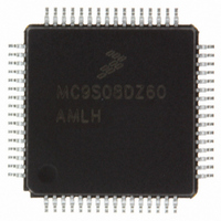
MC9S08DZ60MLC Freescale Semiconductor, MC9S08DZ60MLC Datasheet - Page 344

MC9S08DZ60MLC
Manufacturer Part Number
MC9S08DZ60MLC
Description
IC MCU 60K FLASH 4K RAM 32-LQFP
Manufacturer
Freescale Semiconductor
Series
HCS08r
Specifications of MC9S08DZ60MLC
Core Processor
HCS08
Core Size
8-Bit
Speed
40MHz
Connectivity
CAN, I²C, LIN, SCI, SPI
Peripherals
LVD, POR, PWM, WDT
Number Of I /o
25
Program Memory Size
60KB (60K x 8)
Program Memory Type
FLASH
Eeprom Size
2K x 8
Ram Size
4K x 8
Voltage - Supply (vcc/vdd)
2.7 V ~ 5.5 V
Data Converters
A/D 10x12b
Oscillator Type
External
Operating Temperature
-40°C ~ 125°C
Package / Case
32-LQFP
For Use With
DEMO9S08DZ60 - BOARD DEMOEVB9S08DZ60 - BOARD EVAL FOR 9S08DZ60
Lead Free Status / RoHS Status
Lead free / RoHS Compliant
Available stocks
Company
Part Number
Manufacturer
Quantity
Price
Company:
Part Number:
MC9S08DZ60MLC
Manufacturer:
Freescale Semiconductor
Quantity:
10 000
- Current page: 344 of 416
- Download datasheet (5Mb)
Chapter 16 Timer/PWM Module (S08TPMV3)
344
5. Center-Aligned PWM
6. Write to TPMxMODH:L registers in BDM mode
7. Update of EPWM signal when CLKSB:CLKSA = 00
— Center-Aligned PWM
— TPMxCnVH:L = TPMxMODH:L [SE110-TPM case 1]
— TPMxCnVH:L = (TPMxMODH:L - 1) [SE110-TPM case 2]
— TPMxCnVH:L is changed from 0x0000 to a non-zero value [SE110-TPM case 3 and 5]
— TPMxCnVH:L is changed from a non-zero value to 0x0000 [SE110-TPM case 4]
Registers
In the TPM v3 a write to TPMxSC register in BDM mode clears the write coherency mechanism
of TPMxMODH:L registers. Instead, in the TPM v2 this coherency mechanism is not cleared when
there is a write to TPMxSC register.
In the TPM v3 if CLKSB:CLKSA = 00, then the EPWM signal in the channel output is not update
(it is frozen while CLKSB:CLKSA = 00). Instead, in the TPM v2 the EPWM signal is updated at
the next rising edge of bus clock after a write to TPMxCnSC register.
The
after the reset (CLKSB:CLKSA = 00) and if there is a write to TPMxCnSC register.
TPM counter changes from (TPMxMODH:L - 1) to (TPMxMODH:L). If the TPM counter is
a free-running counter, then this update is made when the TPM counter changes from $FFFE
to $FFFF. Instead, the TPM v2 makes this update after that the both bytes were written and
when the TPM counter changes from TPMxMODH:L to $0000.
In this mode and if (CLKSB:CLKSA not = 00), the TPM v3 updates the TPMxCnVH:L
registers with the value of their write buffer after that the both bytes were written and when the
TPM counter changes from (TPMxMODH:L - 1) to (TPMxMODH:L). If the TPM counter is
a free-running counter, then this update is made when the TPM counter changes from $FFFE
to $FFFF. Instead, the TPM v2 makes this update after that the both bytes were written and
when the TPM counter changes from TPMxMODH:L to (TPMxMODH:L - 1).
In this case, the TPM v3 produces 100% duty cycle. Instead, the TPM v2 produces 0% duty
cycle.
In this case, the TPM v3 produces almost 100% duty cycle. Instead, the TPM v2 produces 0%
duty cycle.
In this case, the TPM v3 waits for the start of a new PWM period to begin using the new duty
cycle setting. Instead, the TPM v2 changes the channel output at the middle of the current
PWM period (when the count reaches 0x0000).
In this case, the TPM v3 finishes the current PWM period using the old duty cycle setting.
Instead, the TPM v2 finishes the current PWM period using the new duty cycle setting.
Figure 0-1
(TPMxMODH:TPMxMODL))
and
Figure 0-2
(Section 16.4.2.4, “Center-Aligned PWM
(Section 16.4.2.4, “Center-Aligned PWM
MC9S08DZ60 Series Data Sheet, Rev. 4
show when the EPWM signals generated by TPM v2 and TPM v3
(Section 16.3.3, “TPM Counter Modulo
Mode)
Mode)
Freescale Semiconductor
Related parts for MC9S08DZ60MLC
Image
Part Number
Description
Manufacturer
Datasheet
Request
R
Part Number:
Description:
Manufacturer:
Freescale Semiconductor, Inc
Datasheet:
Part Number:
Description:
Manufacturer:
Freescale Semiconductor, Inc
Datasheet:
Part Number:
Description:
Manufacturer:
Freescale Semiconductor, Inc
Datasheet:
Part Number:
Description:
Manufacturer:
Freescale Semiconductor, Inc
Datasheet:
Part Number:
Description:
Manufacturer:
Freescale Semiconductor, Inc
Datasheet:
Part Number:
Description:
Manufacturer:
Freescale Semiconductor, Inc
Datasheet:
Part Number:
Description:
Manufacturer:
Freescale Semiconductor, Inc
Datasheet:
Part Number:
Description:
Manufacturer:
Freescale Semiconductor, Inc
Datasheet:
Part Number:
Description:
Manufacturer:
Freescale Semiconductor, Inc
Datasheet:
Part Number:
Description:
Manufacturer:
Freescale Semiconductor, Inc
Datasheet:
Part Number:
Description:
Manufacturer:
Freescale Semiconductor, Inc
Datasheet:
Part Number:
Description:
Manufacturer:
Freescale Semiconductor, Inc
Datasheet:
Part Number:
Description:
Manufacturer:
Freescale Semiconductor, Inc
Datasheet:
Part Number:
Description:
Manufacturer:
Freescale Semiconductor, Inc
Datasheet:
Part Number:
Description:
Manufacturer:
Freescale Semiconductor, Inc
Datasheet:


